Semiconductor device and its manufacturing method
a technology of semiconductor devices and manufacturing methods, applied in semiconductor devices, semiconductor/solid-state device details, electrical apparatus, etc., can solve problems such as the inability to solve problems by etching techniques, and achieve the effect of reducing the leak current of inter-layer insulating films and improving the reliability of semiconductor devices
- Summary
- Abstract
- Description
- Claims
- Application Information
AI Technical Summary
Benefits of technology
Problems solved by technology
Method used
Image

Examples
first embodiment
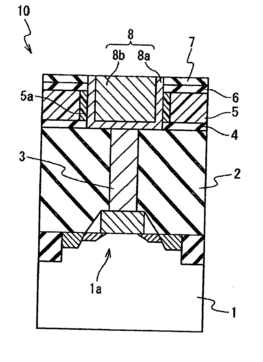
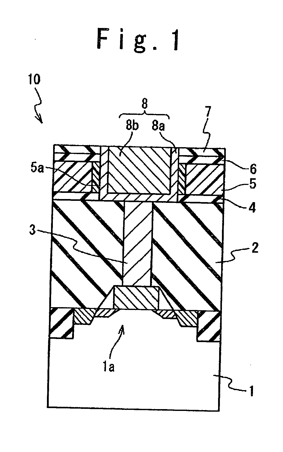
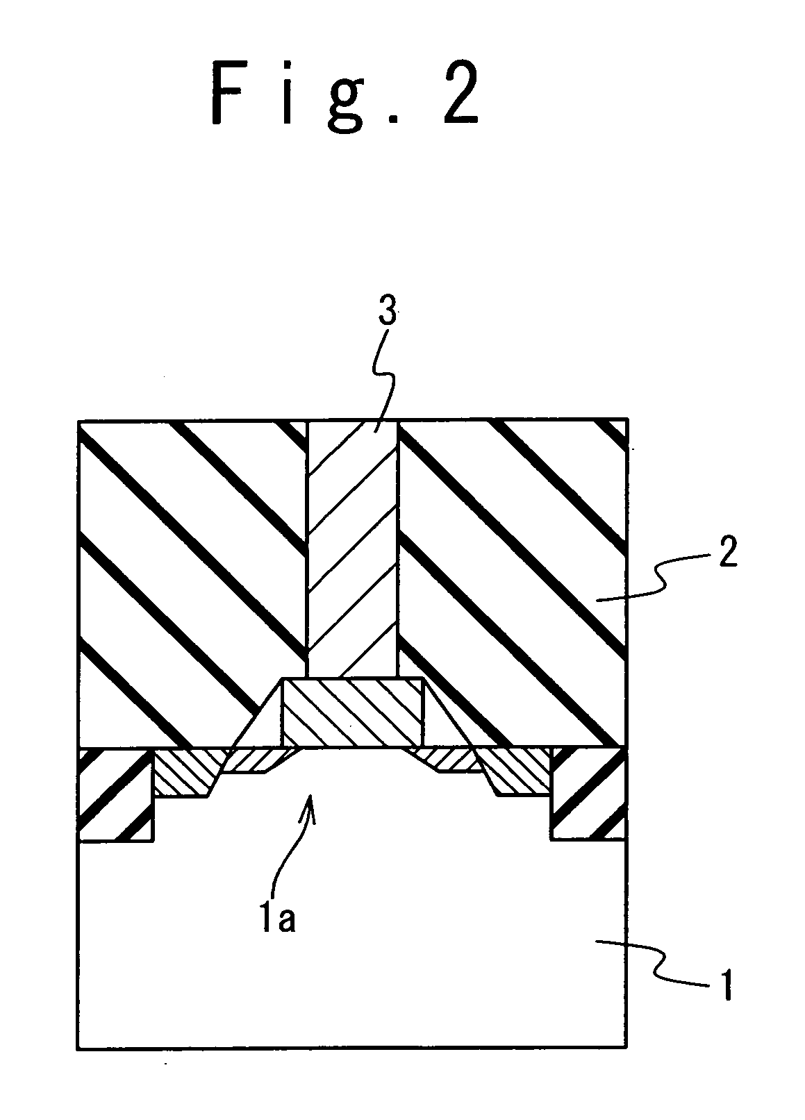
[0086]FIG. 1 shows a semiconductor device 10 of the first embodiment of the present invention. The semiconductor device 10 has a semiconductor substrate 1 in which a MOS transistor 1a is formed on the surface. The semiconductor substrate 1 is covered with an inter-layer insulating film 2. A conductive plug 3 is formed in the inter-layer insulating film 2 to pass through the inter-layer insulating film 2 to the MOS transistor 1a.
[0087] A silicon nitride film 4, an organic insulating film 5, a silicon oxide film 6 and a silicon nitride film 7 are sequentially formed on the inter-layer insulating film 2. The silicon nitride film 4 is an etching stopper used in etching the organic insulating film 5. The organic insulating film 5 is made of organic low dielectric constant material whose dielectric constant is low, and it is typically made of the di-vinyl-siloxane benzo cyclobutene (BCB) polymer. The dielectric constant of the organic insulating film 5 made of the BCB film is between 2.4...
second embodiment
[0130] In the second embodiment, the technique for adding the nitrogen and growing the modified layer on the sidewall of the organic insulating film is applied to a dual damascene process.
[0131]FIG. 14 shows a semiconductor device 20 according to the second embodiment of the present invention. The semiconductor device 20 has a substrate 21 and a lower wiring structure 22 formed on the substrate 21. Although MOS transistors and plugs are formed on the substrate 21, all of them are not shown. The lower wiring structure 22 includes a laminated insulating film 23 and a copper wiring 24. The copper wiring 24 is embedded in a wiring groove formed in the laminated insulating film 23.
[0132] On the lower wiring structure 22, a cap film 25 and an organic interlayer film 26 are sequentially formed. The cap film 25 is formed of a silicon nitride film. The organic interlayer film 26 is formed of an organic low dielectric constant material whose dielectric constant is low, and it is typically f...
third embodiment
[0157] In the third embodiment, the semiconductor device 20 of the second embodiment is formed by a so-called [Dual Hard Mask Process] and not by the [Via First Process].
[0158] At first, similarly to the second embodiment, after the lower wiring structure 22 shown in FIG. 15 is formed on the substrate 21, as shown in FIG. 16, the cap film 25, the organic interlayer film 26, the stopper film 27, the organic interlayer film 28 and the hard mask film 29 are formed. As mentioned above, the cap film 25, the stopper film 27 and the hard mask film 29 are formed of the silicon nitride film, and the organic interlayer film 26 and the organic interlayer film 28 are formed of the organic low dielectric constant material.
[0159] As described later, in the third embodiment, the organic interlayer film 26 and the organic interlayer film 28 require the usage of the material which enables the selective etching to the photo resist and the reflection protecting film. Typically, for the organic inter...
PUM
 Abstract
Description
Claims
Application Information
 - R&D Engineer
- R&D Manager
- IP Professional
- Industry Leading Data Capabilities
- Powerful AI technology
- Patent DNA Extraction
Browse by: Latest US Patents, China's latest patents, Technical Efficacy Thesaurus, Application Domain, Technology Topic.
© 2024 PatSnap. All rights reserved.Legal|Privacy policy|Modern Slavery Act Transparency Statement|Sitemap