
CMOS image sensor for high speed signal processing

a high-speed signal processing and image sensor technology, applied in the field of cmos image sensors, can solve the problems of difficult to achieve signal stability, difficult to design functional blocks to operate at high speed, and the processing speed of the corresponding path must be very fast, so as to achieve the effect of eliminating offset differences and ensuring signal stability

Active Publication Date: 2005-11-17
INTELLECTUAL VENTURES II
View PDF13 Cites 22 Cited by
  • Summary
  • Abstract
  • Description
  • Claims
  • Application Information

AI Technical Summary

Benefits of technology

[0013] It is, therefore, an object of the present invention to provide a CMOS image sensor, in which signal stability can be ensured using the low-speed functional blocks, while maintaining an entire signal processing speed. Further, it is possible to effectively remove the offset difference with respect to the same color signals, which may occur due to the multi-paths.

Problems solved by technology

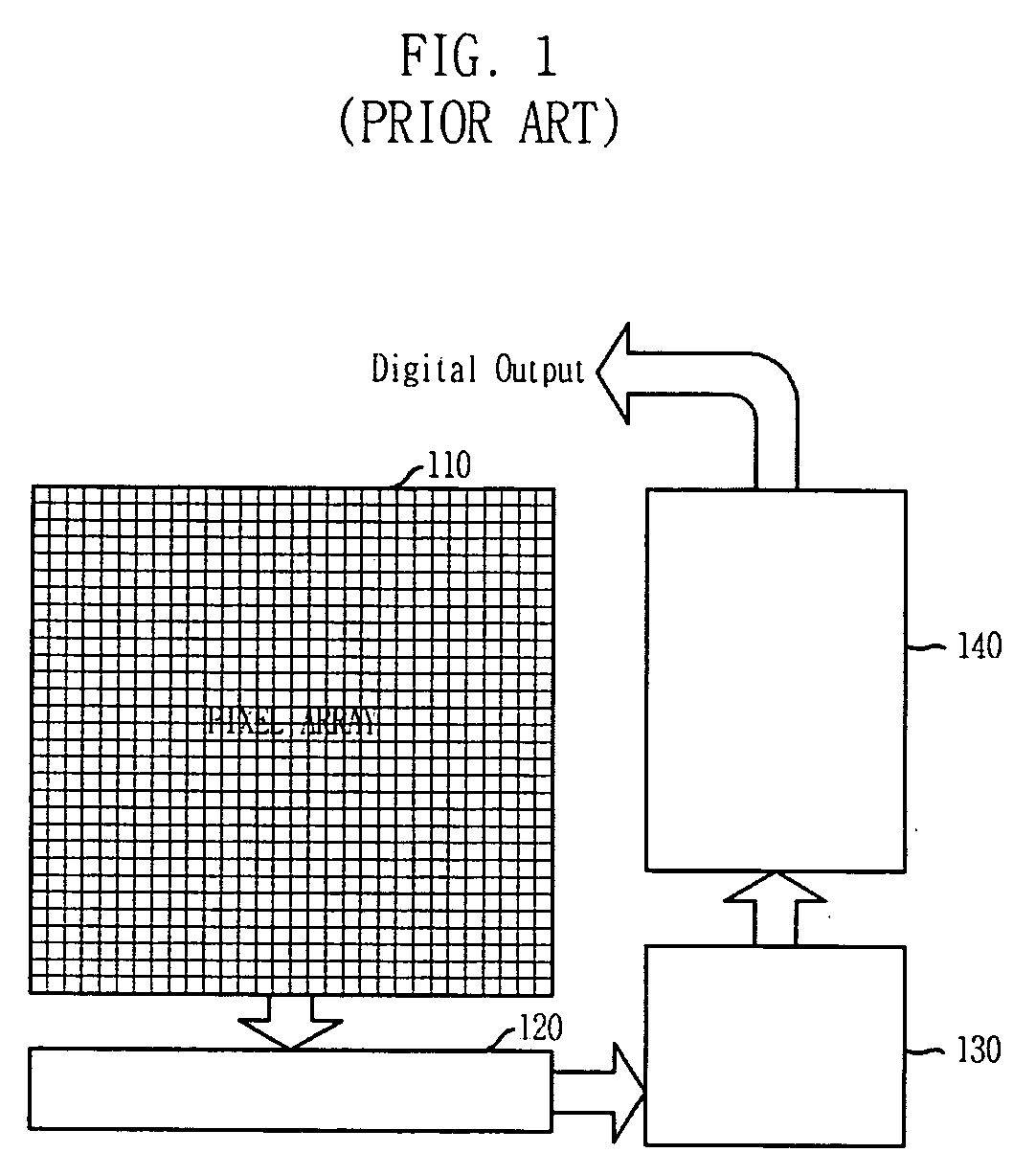
However, when a large amount of data is processed through the single path, a processing speed of the corresponding path must be very fast.
However, it is difficult to design the functional blocks to operate at high speed.
Also, it is difficult to obtain signal stability.
Consequently, reliability and productivity of the device may be badly affected.

Method used


Image

  • CMOS image sensor for high speed signal processing
  • CMOS image sensor for high speed signal processing
  • CMOS image sensor for high speed signal processing

Examples


Embodiment Construction

[0023] Hereinafter, the present invention will be described in detail with reference to the accompanying drawings.

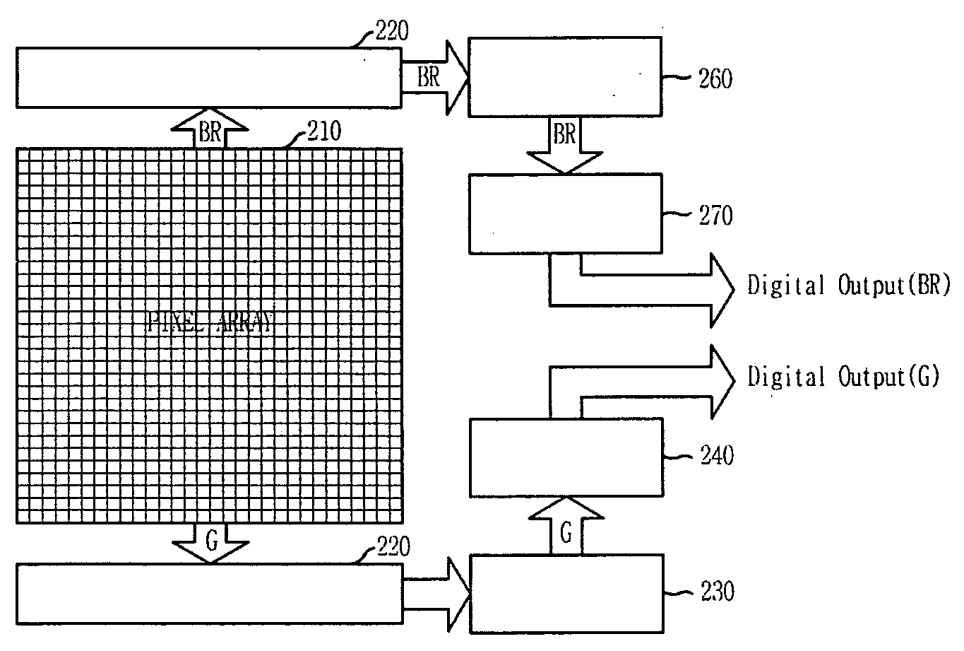
[0024] In accordance with the present invention, analog signals are processed through multi-paths so as to ensure a signal stability using low-speed functional blocks, while maintaining an entire signal processing speed. Also, offset values existing on respective paths are previously read through dummy pixels where light is shielded, and their average value is stored. When signals are outputted from effective pixels, the value is removed for each path. In this manner, the offset values that occur when the same color signals within the pixel array are processed through different paths can be effectively removed.

[0025]FIG. 3 is a block diagram of a CMOS image sensor in accordance with an embodiment of the present invention.

[0026] Referring to FIG. 3, analog signals outputted from pixels are parallel processed. That is, a G-path 220, 230 and 240 processes signals of G pi...


PUM


Abstract

A CMOS image sensor includes: a plurality of CDS / PGAs (correlating double sampling / programmable gain amplifiers) for processing output signals of pixels corresponding to same colors on different paths; and an offset difference removing part for removing offset difference that occurs when the same color signals are processed on the different paths, wherein the offset difference removing part includes: a dummy pixel array where light is shielded; a unit for reading signals of the dummy pixel array through the CDS / PGAs and storing average offset values for each path; and a signal synthesizing unit for synthesizing the average offset values and signals of an effective pixel array, which are read through the respective CDS / PGAs, and outputting signals of which offset difference is removed.

Description

FIELD OF THE INVENTION [0001] The present invention relates to a CMOS image sensor; and, more particularly, to a CMOS image sensor for high speed signal processing and a signal processing method therefor. DESCRIPTION OF RELATED ART [0002] An image sensor is an apparatus to convert an optical image into an electrical signal. Such an image sensor is largely classified into a complementary metal oxide semiconductor (CMOS) image sensor and a charge coupled device (CCD). [0003] In the case of the CCD, individual MOS capacitors are disposed very close to one another and charge carriers are stored in the capacitors and transferred. Meanwhile, in the case of the CMOS image sensor, a pixel array is constructed using a technology of fabricating CMOS integrated circuit and output data are detected in sequence through a switching operation. Since the CMOS image sensor has an advantage of low power consumption, it is widely used in a personal communication system, such as a hand-held phone. [000...

Claims


Application Information

Patent Timeline
Patent Type & Authority Applications(United States)
IPC IPC(8): H01L27/146H01L27/14H04N23/12H04N25/00
CPCH04N5/361H04N9/045H04N5/3742H04N5/3728H04N25/73H04N25/70H04N25/767H04N25/134H04N25/78H04N25/633H04N25/63
Inventor KIM, NAM-RYEOLKIM, SONG-YIBAE, CHANG-MINOH, HACK-SOO
Owner INTELLECTUAL VENTURES II
Learn More