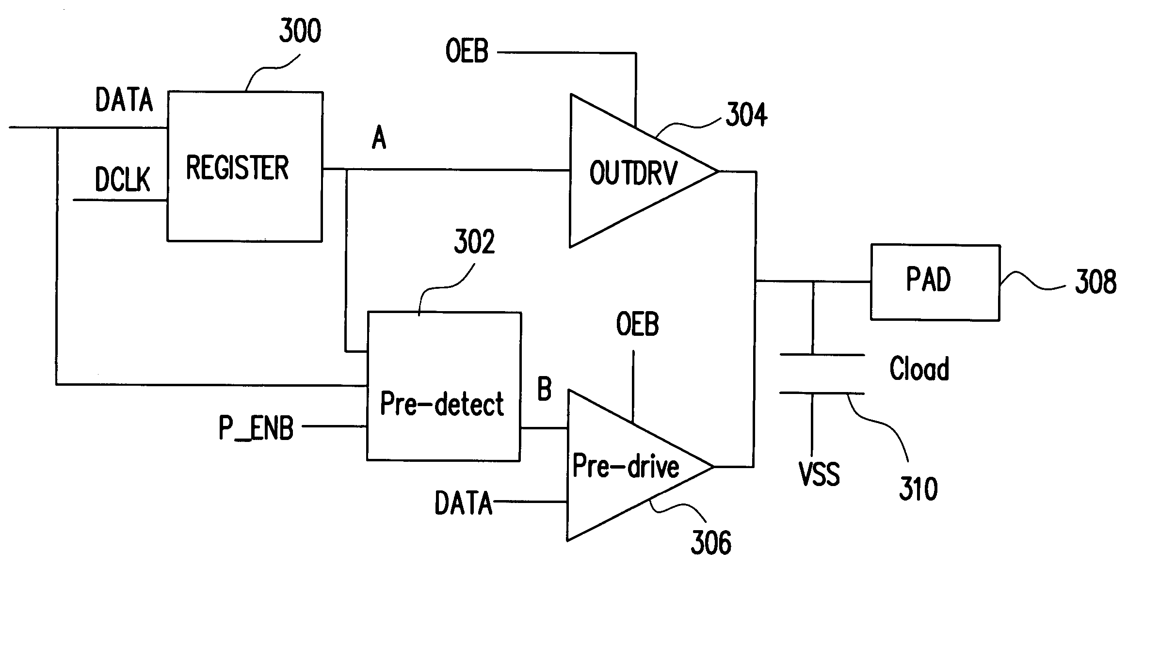
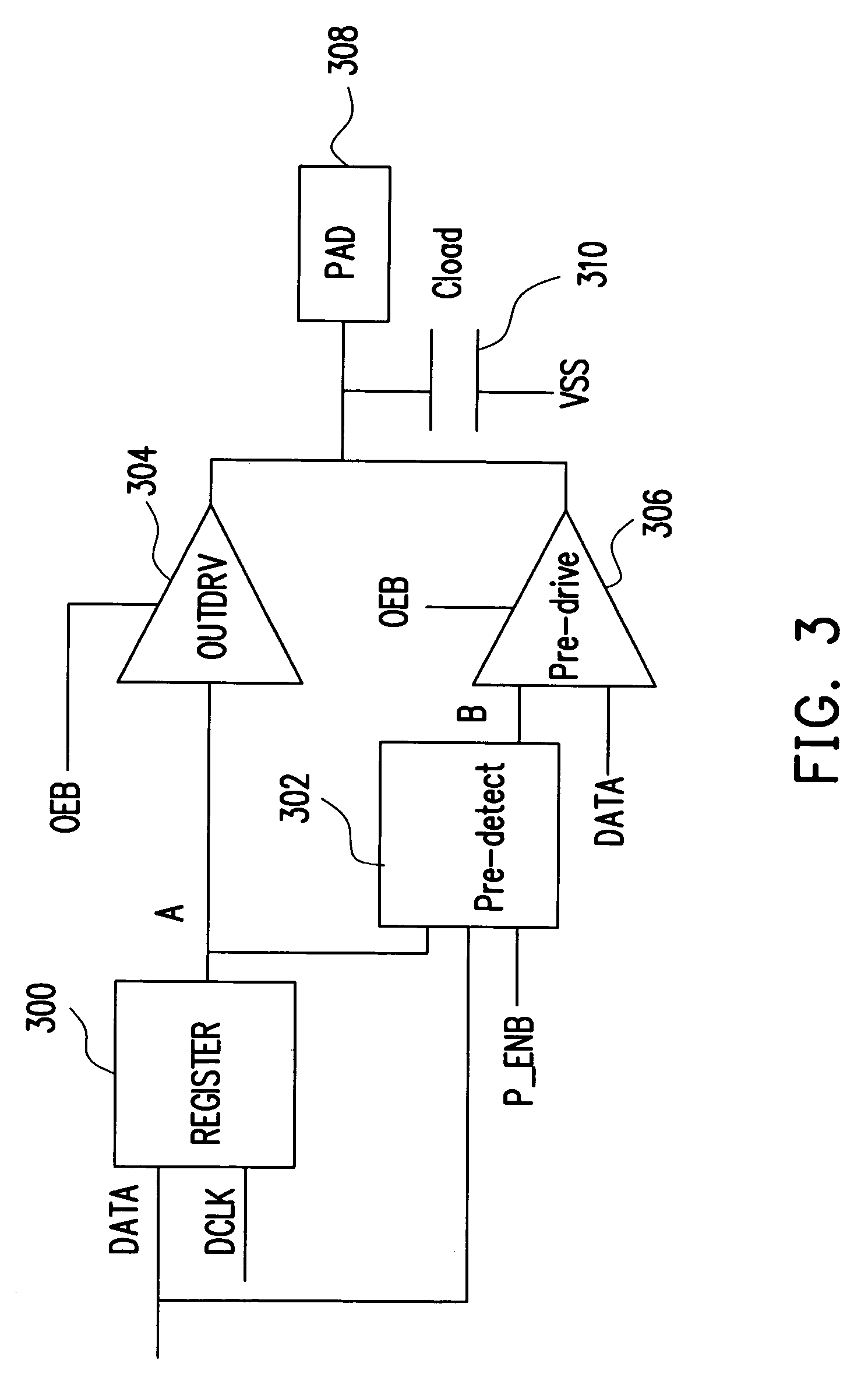
[0022] In the invention, a novel memory I/O driving circuit is proposed. In the present invention, a pre-driving circuit is used to at least adjust the rising edge and the falling edge of the data signal at the I/O pad. Due to the pre-driving effect, the signal edges at the first part have been adjusted to be more horizontal. This at least allows the data can be keep longer with more hold time with reduced errors if the host timing is shifted.
[0023]FIG. 3 is block diagram, schematically illustrating the memory-card driving circuit for driving multiple I/O pads in a memory card, according to an embodiment of the invention. In FIG. 3, the memory-card driving circuit of the invention includes a register 300, a pre-detecting circuit 302, an output driving circuit (OUTDRV) 304, a pre-driving circuit 306. In addition, an I/O pad 308 is coupled to the output terminals of the output driving circuit (OUTDRV) 304 and the pre-driving circuit 306. However, a load capacitor 310 and a circuit load impedance (not shown) between the pad 308 and a system low voltage source, such as a ground voltage VSS.
[0024] The register 300 receives the data (DATA) and a delayed clock (DCLK). The delayed clock has a delay to a clock (CLK). Then, the data is shifted out as the signal A. The signal A and the data (DATA) are sent to the pre-detecting circuit 302, which is also controlled by the enable signal P_ENB. At the same time, the signal A is sent to the output driver 304. The output driver 304 can be similar to the conventional driver and is controlled by the enable signal OEB. Then, the output signal is sent to the I/O pad 308.
[0025] Also referring to FIG. 4, in the invention, the pre-detecting circuit 302 compares the new-coming data signal DATA and the currently-existing data, indicated by signal A, and then exports the signal B. The signal B is fed to the pre-driving circuit 306. For the signal B, when the currently-existing data and the new-coming data are the same, then pre-driving circuit 306 is disabled, such as a low level. Otherwise, the pre-driving circuit 306 is enabled, such as high level, to pre-drive the new-coming data after the rising edge of the clock CLK. However, the control signal P_ENB can enable or disable the pre-detecting circuit 302. When the pre-detecting circuit 302 is disabled, the pre-driving circuit 306 becomes the high-impedance state. In other words, the pre-driving circuit 306 is off and the data is driven similar to the conventional way as shown in FIG. 1.
[0026] The pre-driving circuit 306 can also receive the DATA in operation, and is controlled by the enable signal OEB. The output terminals of the output driver 304 and the pre-driving circuit 306 are coupled together to a common node. The load capacitor 310 exists between the pad 308 and the system low voltage Vss. The common node is, for example, the I/O pad 308. When the pre-diving circuit 306 is enabled, the circuit provides an output impedance, which is incorporated with the output impedance from the output driver 304. As a result, the total impedance is changed. According to the properties of RC circuit, the slops of the rising edge and the falling data for the signal arriving at the I/O pad 308. The slop change can be seen in FIG. 4. As a result, the rising edge or the falling edge has two edge parts. The first edge pat, within a time period, has the absolute slop, more closing to the horizontal level. When the pre-driving circuit 306 is disabled, the RC constant for the circuit returns back to the original setting.
[0027] Therefore, when the voltage level on the pad 308 is read, for example, at the falling edge of the clock CLK, the data can be held by the time period. Even if the timing has been shifted a little, the data still can be possibly read with reduced error.
[0028] For the circuit in FIG. 3, the pre-detecting circuit 302 can be implemented by a circuit, such as the circuit in FIG. 5. In FIG. 5, the pre-detecting circuit 302 may include an XOR (exclusive OR) logic gate 500 and an AND logic gate 502, wherein the XOR logic gate 500 can be replaced by XNOR (exclusive NOR) logic gate in an equivalent operation. The XOR logic gate 500 is the example for descriptions. The XOR logic gate 500 receives the data DATA and the signal A. The output of the XOR logic gate 500 is exported to the AND logic gate 502 while the control signal P_ENG is also fed for controlling the pre-detecting circuit 302. The AND logic gate 502 the exports the signal B.
[0029] The pre-driving circuit 306 is also shown in FIGS. 6A-6C, as an example for circuit implementation. Before describing the better detail circuit in FIG. 6A, the control signals are branched as shown in FIGS. 6B and 6C. In FIG. 6B, the control signal OEB is branched into a control signal OUT_EN and another control signal OUT_E, which are complementary in logic states. Similarly, the data signal DATA is branched into the control signal P_DET for controlling the P-type MOS transistors and the control signal N_DET fort controlling the N-type MOS transistors. The branching circuits in FIG. 6B and FIG. 6C can simply be two inverters in cascade connection.
[0030] The pre-driving circuit 306 basically includes one part from P-type MOS devices and another part from N-type MOS devices. The pre-driving circuit 306, for example, includes a first inverter 600, receiving the output signal B from the pre-detecting circuit 302. An NOR logic gate 602a receives the control signal OUT_EN, an output from the inverter 600, and a feedback signal from the common node, which is from the I/O pad 308. Another inverter 604a receives an output from the NOR logic gate 602a. A P-type MOS transistor 606a has a gate coupled to an output terminal of the second inverter 604a, a first source/drain (S/D) electrode coupled to the I/O pad 308, and a second S/D electrode. Here, the MOS transistor has the source electrode and the drain electrode, which are interchangeable depending the actual operation. Another P-type MOS transistor 608a has a gate receiving the control signal P_DET, a first S/D electrode coupled to a system high voltage source VDD, and a second S/D electrode coupled with the second S/D electrode of the P-type MOS transistor 606a. A NAND logic gate 602b receives the control signal OUT_E, the output from the signal B, and the feedback signal from the I/O pad 308. Another inverter 604b receives an output from the NAND logic gate 602b. An N-type MOS transistor 606b has a gate receiving an output from the inverter 604b, a first S/D electrode coupled to the I/O pad 308, and a second S/D electrode. Another N-type MOS transistor 608b has a gate receiving the control signal N_DET, a first S/D electrode coupled to a system low voltage source VSS, such as ground, and a second S/D electrode coupled with the second S/D electrode of the N-type MOS transistor 606b.
[0031] Alternatively, the memory-card driving circuit, as shown in FIG. 3, can be modified into the circuit shown in FIG. 7. In FIG. 7, the memory-card driving circuit may include a register 700, a pre-detecting circuit 702, an output driving circuit (OUTDRV) 704, a pre-driving circuit 706. In addition, an I/O pad 708 is coupled to the output terminals of the output driving circuit (OUTDRV) 704 and the pre-driving circuit 706. However, a load capacitor 710 and a circuit load impedance (not shown) between the pad 308 and a system low voltage source, such as a ground voltage VSS.
[0032] In this example, the output signal from the pre-detecting circuit 702 is also fed to the output driver 704. For this design, the circuit for pre-driving circuit 706 may be designed as shown in FIGS. 8A-8B.
[0033] In FIG. 7, the pre-driving circuit 706 receives the signal B from the pre-detecting circuit 702. In FIG. 8A, the pre-driving circuit 706 also receives the control signal OEB, which is branched into two complementary control signals OUT_E and OUT_EN by a way, for example, shown in FIG. 8B. An NAND logic gate 802a receives the control signal OUT_EN, signal DATA and the signal B. An operational amplifier (OP) 804a has an input terminal VB receiving a reference signal VREF, while a second input terminal VA coupled to the I/O pad PAD. A first P-type MOS transistor 806a has a gate coupled to the output terminal of the OP 804a, a first S/D electrode coupled to the I/O pad PAD, and a second S/D electrode. A second P-type MOS transistor 808a has a gate coupled to an output terminal of the NAND logic gate 802a, a first S/D electrode coupled to a system high voltage source VDD, and a second S/D electrode coupled with the second S/D electrode of the first P-type MOS transistor 806a.
[0034] For the N-type MOS devices in the pre-driving circuit, it includes a NOR logic gate 802b receives the control signal OUT_E, signal DATA, and the output from the inverter 800. The inverter 800 receives the signal B. Another operational amplifier 804b has a first input terminal VA coupled to the PAD, a second input terminal VB receiving the reference signal. A first N-type MOS transistor 806b has a gate coupled to the output terminal of the OP 804b, a first S/D electrode coupled to the PAD, and a second S/D electrode. A second N-type MOS transistor 808b has a gate coupled to an output terminal of the NOR logic gate 802b, a first S/D electrode coupled to the system low voltage source VSS, and a second S/D electrode coupled with the second S/D electrode of the first N-type MOS transistor 806b.
[0035] The invention have achieved several advantages at least as follows:
[0036] With the pre-detect circuit, it can reduce the output transient glitch, in order to minimize the transient current on I/O driver. The pre-detecting circuit can decide the on/off state for the pre-driving circuit. The pre-driving circuit can keep the output at the exist state (TTL level) for getting a maximum hold time, but the trend is applied to next coming data. The invention provides a first stage driving capability and the level detection circuit to reduce IO transient current and speed up IO transient time.
[0037] It will be apparent to those skilled in the art that various modifications and variations can be made to the structure of the present invention without departing from the scope or spirit of the invention. In view of the foregoing, it is intended that the present invention covers modifications and variations of this invention provided they fall within the scope of the following claims and their equivalents.