Method of controlling the film properties of PECVD-deposited thin films

a technology of pecvd and thin films, applied in plasma techniques, solid-state diffusion coatings, coatings, etc., can solve the problems of non-uniform film thickness of precursor source gas, and achieve the effect of increasing the surface area, and increasing the hollow cathode

Active Publication Date: 2005-11-17
APPLIED MATERIALS INC
View PDF35 Cites 512 Cited by
  • Summary
  • Abstract
  • Description
  • Claims
  • Application Information

AI Technical Summary

Benefits of technology

[0052] We have discovered that control of plasma density distribution over the substrate surface can be achieved, for example (and not by way of limitation), by equipment modifications, such as by modifying openings in the gas distribution diffuser plate so that there is an increase in hollow cathode effect from the center toward the edge of the diffuser plate. This increase in hollow cathode effect may be provided by gradually increasing diameters or depths, or combinations thereof, of the openings (hollow cathode cavities) from the center toward the edge of the diffuser plate. By increasing either the volume of the hollow cathode cavity from the center toward the edge of the diffuser plate or the number of gas passages present from the center toward the edge of the diffuser plate, hollow cathode effect is increased in this direction. This provides an increased surface area for hollow cathode cavity effect from the center toward the edge of the diffuser plate. To further increase the hollow cathode effect, the ratio of surface area to volume of the cavity may be increased. The increased hollow cathode effect adjusts the plasma density so that more uniformity is achieved from center to edge of the substrate. We have found that, by increasing the hollow cathode effect from the center toward the edge of the diffuser plate, modifications to other PECVD process variables, such as the precursor gas recipe may not be necessary to obtain a uniform film deposition.
[0053] A number of diffuser plate designs may be used to provide increased hollow cathode effect. In one embodiment, a gas dist

Problems solved by technology

However, we discovered that when the substrate size was increased to dimensions of 1500 mm to 1800 mm, this precursor source gas produced a non-uniform film thickness which varied by as much as about 25%; produ

Method used


Image

  • Method of controlling the film properties of PECVD-deposited thin films
  • Method of controlling the film properties of PECVD-deposited thin films
  • Method of controlling the film properties of PECVD-deposited thin films

Examples


example one

PECVD Deposition of a-SiNx:H Gate Dielectric Layers by Increasing the Concentration of NH3 in the Precursor Gas Composition

[0185] We have previously described all of the performance requirements for the a-SiNx:H gate dielectric layer. We carried out extensive experimentation in an effort to produce a PECVD deposited a-SiNx:H gate dielectric layer which met the performance requirements and which provided a uniformity in film thickness and uniformity in film properties, including structural and chemical composition, when PECVD deposited over a large surface area, larger than 1000 mm×1000 mm, for example. One basic requirement is that the a-SiNx:H film deposition rate is more than 1000 Å / min, and typically more than 1300 Å / min, so that the fabrication throughput for the TFT provides adequate productivity to be economically competitive. The basic requirements for the a-SiNx:H film are that: the Si—H bonded content of the a-SiNx:H film is less than about 15 atomic %; the film stress ran...

example two

PECVD Deposition of a-SiNx:H Gate Dielectric Layers of Uniform Thickness by Controlling a Combination of Process Parameters, using the AKT™ 25 KA PECVD System

[0205] As discussed above, we have discovered that controlling a combination of PECVD deposition process parameters during deposition of silicon-containing thin film provides improved control over surface standing wave effects. These process parameters include: the spacing between the upper and lower electrodes in the plasma reactor; the RF frequency of the plasma source; the RF power to the plasma source; the process chamber pressure; and the relative concentrations of the various components in the precursor gas composition.

[0206] We performed a series of experiments to determine the advantageous ranges for each process parameter, in order to provide maximum control over surface standing wave effects and uniformity of film properties (especially film thickness). A comparison between film uniformity available prior to the pre...

example three

Modification of the Diffuser Plate of the Gas Distribution Assembly

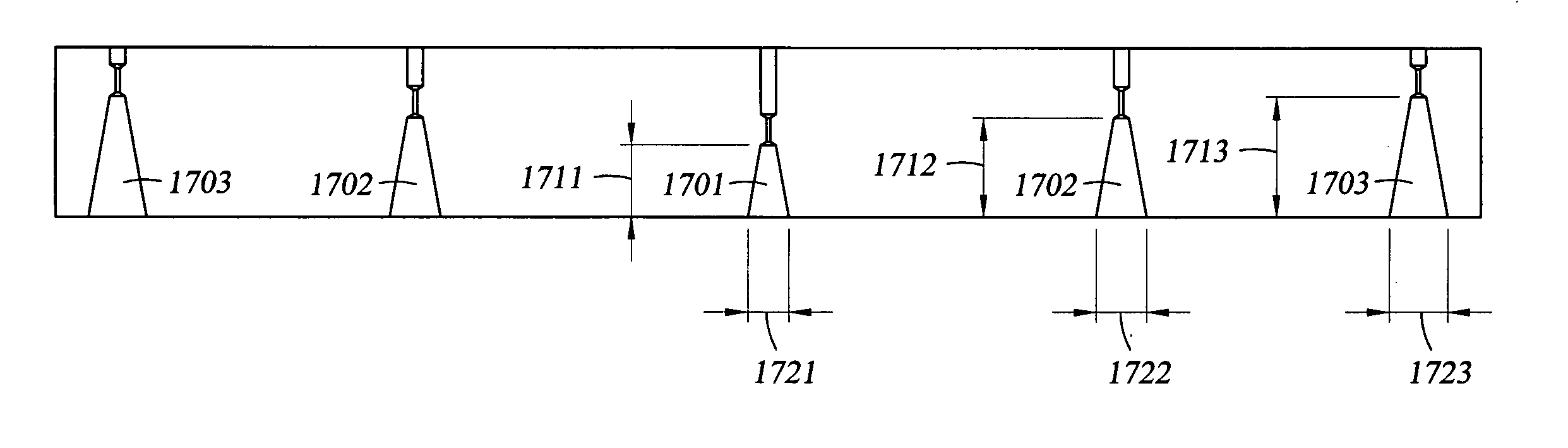
[0219] We found that, as substrate sizes increased over 30,000 cm2, to 40,000 cm2 and beyond, process modifications such as those described in Examples One and Two, above, are not always enough to compensate for surface standing wave effects. For example, FIG. 20 is a graph 2000 of the film thickness 2002 as a function of the distance of travel 2004 (in mm) across the width of the substrate, where the width of the substrate was 2200 mm and the length of the substrate was 1870 mm (for a total substrate area of 41,140 cm2), for an a-SiNx:H film. The a-SiNx:H film was PECVD deposited in an AKT™ 40 K PECVD System (which is described above in “APPARATUS FOR PRACTICING THE INVENTION” and shown schematically in FIGS. 19A-19C) process chamber having an electrode spacing of 600 mils, using a “standard” (uniform hollow cathode cavity) diffuser plate.

[0220] We discovered that controlling the plasma density at point locations ...


PUM

PropertyMeasurementUnit
Temperatureaaaaaaaaaa

Abstract

We have discovered methods of controlling a combination of PECVD deposition process parameters during deposition of thin films which provides improved control over surface standing wave effects which affect deposited film thickness uniformity and physical property uniformity. By minimizing surface standing wave effects, the uniformity of film properties across a substrate surface onto which the films have been deposited is improved. In addition, we have developed a gas diffusion plate design which assists in the control of plasma density to be symmetrical or asymmetrical over a substrate surface during film deposition, which also provides improved control over uniformity of deposited film thickness.

Description

RELATED APPLICATIONS [0001] This application claims benefit of priority of the following U.S. patent applications: U.S. application Ser. No. 10 / 962,936, filed Oct. 12, 2004, which is currently pending; U.S. application Ser. No. 10 / 897,775, filed Jul. 23, 2004; U.S. application Ser. No. 10 / 889,683, filed Jul. 12, 2004, which is currently pending; U.S. application Ser. No. 10 / 829,016, filed Apr. 20, 2004, which is currently pending; and, U.S. Provisional Application Ser. No. 60 / 570,876, filed May 12, 2004. Each of the aforementioned application are hereby incorporated by reference in their entireties.BACKGROUND OF THE INVENTION [0002] 1. Field of the Invention [0003] The invention generally relates to a method of controlling process variables during PECVD deposition of a thin film. One important functional result of the variable control is an improvement in the uniformity of film properties of the deposited film across the substrate surface. [0004] 2. Brief Description of the Backgrou...

Claims


Application Information

Patent Timeline
IPC IPC(8): C23C16/00C23C16/34C23C16/509H01J37/32H01L21/316
CPCC23C16/345C23C16/45565C23C16/5096H01L21/31612H01J37/3244H01L21/0217H01L21/02274H01J37/32082
Inventor CHOI, SOO YOUNGWHITE, JOHN M.WANG, QUNHUAPARK, BEOM SOO
Owner APPLIED MATERIALS INC
Why Eureka
Try Eureka