Semiconductor device, method of manufacturing the same, cover for semiconductor device, and electronic equipment

a semiconductor device and semiconductor technology, applied in the direction of basic electric elements, television systems, radio frequency controlled devices, etc., can solve problems such as optical axis distortion, and achieve the effect of eliminating the thickness of adhesives and high degree of precision

Inactive Publication Date: 2005-11-17
SEIKO EPSON CORP
View PDF12 Cites 10 Cited by
  • Summary
  • Abstract
  • Description
  • Claims
  • Application Information

AI Technical Summary

Benefits of technology

[0006] A method of manufacturing a semiconductor device according to the present invention includes the following processes: (a) fixing a cover onto a semiconductor substrate so as to place a surface of the cover that includes a portion defining a first opening face to face on a surface of the semiconductor substrate that includes an electrode; and (b) applying an adhesive to the inside of the first opening. According to the method of the present invention, the adhesive is applied to the first opening of the cover so as to fix the cover onto the semiconductor substrate. This makes it possible to eliminate the thickness of the adhesive between the cover and the semiconductor substrate, since the adhesive stays inside the first opening. At the same time, if the adhesive is applied to the cover being fixed to the semiconductor substrate, the cover can be placed horizontal to the semiconductor substrate with a high degree of precision.

Problems solved by technology

It is also noted that the cover should be mounted horizontally to the optical unit, since the cover fixed in a tilted position on the optical unit may result in distortion of an optical axis.

Method used


Image

  • Semiconductor device, method of manufacturing the same, cover for semiconductor device, and electronic equipment
  • Semiconductor device, method of manufacturing the same, cover for semiconductor device, and electronic equipment
  • Semiconductor device, method of manufacturing the same, cover for semiconductor device, and electronic equipment

Examples


first embodiment

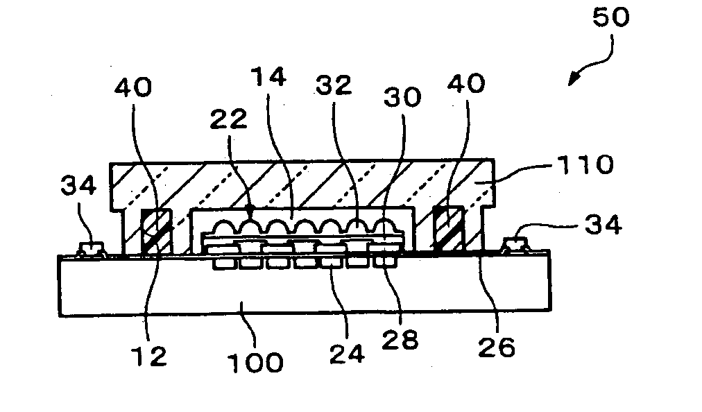
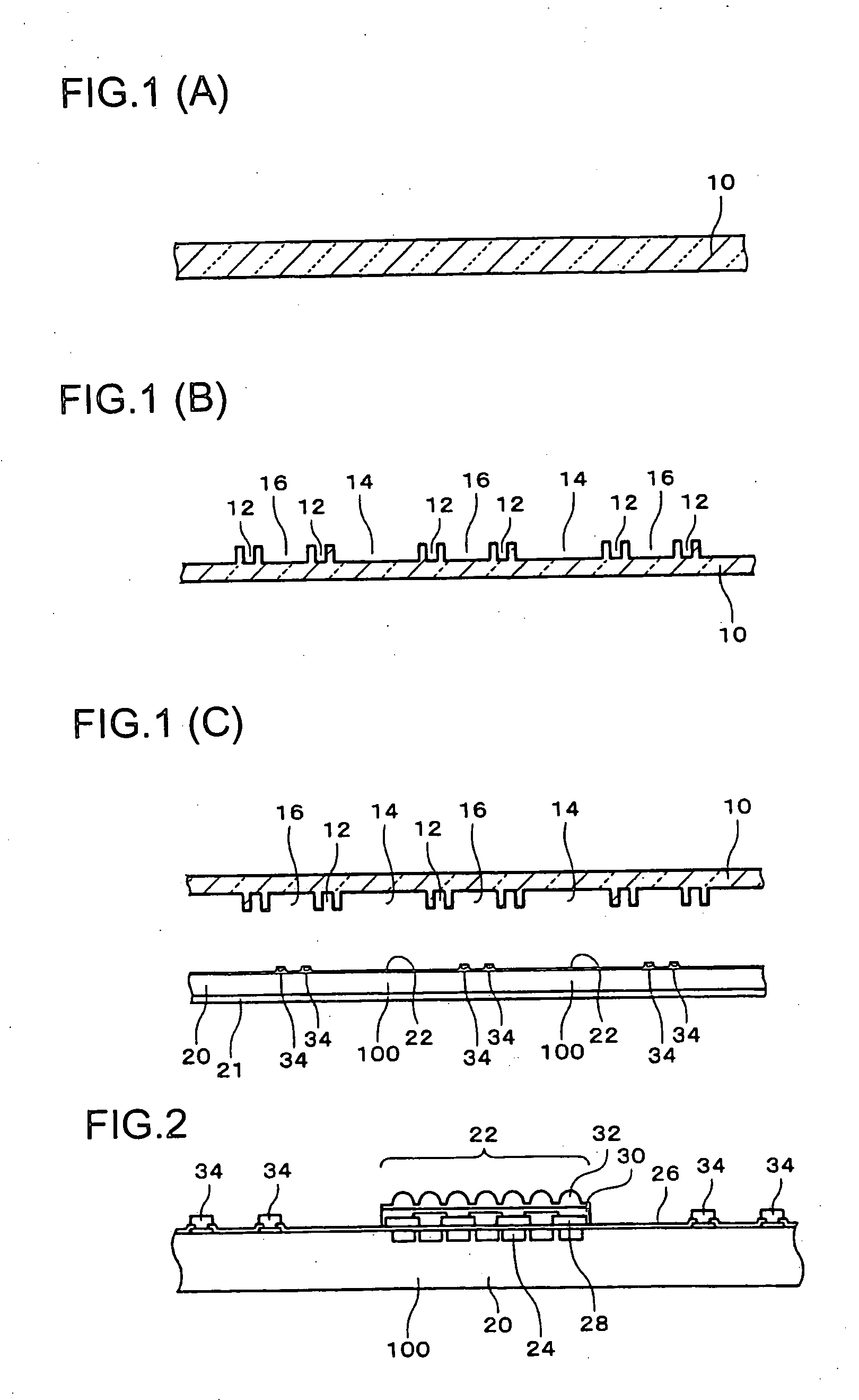
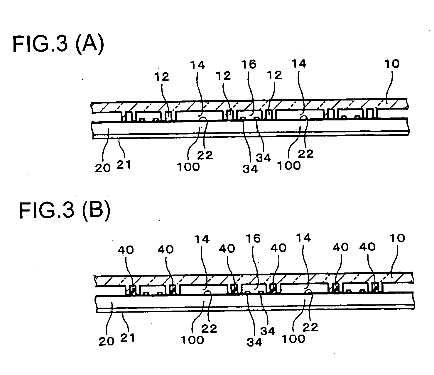
[0040] FIGS. 1 (A) to 6 illustrate a semiconductor device and the method of manufacturing the same according to a first embodiment of the present invention. In this embodiment, an optical device and the method of manufacturing the same are cited as an example. In this method of manufacturing, a cover 10 and a semiconductor substrate 20 are bonded with an adhesive 40. FIG. 4 is a plan view of the cover 10 and the semiconductor substrate 20 facing each other. The semiconductor substrate 20 includes at least one portion (for example, a plurality of such portions) to be an optical chip 100 having an optical unit 22. The semiconductor substrate 20 also includes electrodes 34.

[0041]FIG. 1 (A) shows the cover 10 (a cover for a semiconductor device) used in this embodiment. The cover 10 may be a substrate. The size and the shape of the cover 10 are not limited; it may be as large as the semiconductor substrate 20, and it may be the same shape as the semiconductor substrate 20. As FIG. 4 sh...

second embodiment

[0063] FIGS. 7 (A) to 8 illustrate a method of manufacturing a semiconductor device (e.g. an optical deice) according to a second embodiment of the present invention. FIG. 8 is a plan view of a cover 120 and the semiconductor substrate 20 facing each other.

[0064] In this embodiment, as FIG. 7 (A) shows, the cover 120 includes a portion defining a through-hole 128 that penetrates inside a first opening 122. To put it differently, the cover 120 has the through-hole 128 that extends from the back side of the cover 120, on which the first opening 122 is provided, to the inside of the first opening 122. The through-hole 128 penetrates the cover 120 in the direction of the height of the cover 120. The width of the through-hole 128 may be narrower than that of the first opening 122. The through-hole 128 may be a slit extending to an area overlapping with the first opening 122. For example, as shown in FIG. 8, the first opening 122 here including a plurality of first openings may be arrang...


PUM


Abstract

A method of manufacturing a semiconductor device includes (a) fixing a cover onto a semiconductor substrate so as to place a surface of the cover that includes a portion defining a first opening, face to face on a surface of the semiconductor substrate that includes an electrode and (b) applying an adhesive to the inside of the first opening.

Description

BACKGROUND OF THE INVENTION [0001] 1. Field of the Invention [0002] The present invention relates to a semiconductor device, a method of manufacturing the same, a cover for a semiconductor device and electronic equipment. [0003] 2. Description of Related Art [0004] It is well known that an optical chip that includes an optical unit such as a light receiver should be sealed with a cover on the surface thereof having the optical unit. In sealing the optical chip, a space is left between the optical unit and the cover. When manufacturing a plurality of optical chips by dicing a substrate such as a wafer, substrate shavings resulting from dicing or other wastes may be attached to the optical unit and sealed together without removing the wastes like shavings. It is also noted that the cover should be mounted horizontally to the optical unit, since the cover fixed in a tilted position on the optical unit may result in distortion of an optical axis. [0005] The present invention aims to enh...

Claims


Application Information

Patent Timeline
Patent Type & Authority Applications(United States)
IPC IPC(8): H01L23/04H01L27/146H01L31/0203H01L31/0232
CPCH01L23/04H01L27/14618H01L27/14621H01L27/14625H01L27/14627H01L27/14683H01L27/14685H01L2924/0002H01L31/0203H01L31/0232H01L2924/16235H04N5/2257H01L2924/00H01L31/02327H04N23/57
Inventor OMORI, OSAMU
Owner SEIKO EPSON CORP
Why Eureka
Try Eureka