Method and structure for aligning mechanical based device to integrated circuits

a mechanical based device and integrated circuit technology, applied in the direction of soldering equipment, instruments, photomechanical equipment, etc., can solve the problems of low yield of liquid crystal panels, difficult to make larger, and often bulky crts, etc., to improve the integrated structure, facilitate use, and increase the device yield

Inactive Publication Date: 2005-11-17
MIRADIA INC
View PDF71 Cites 56 Cited by
  • Summary
  • Abstract
  • Description
  • Claims
  • Application Information

AI Technical Summary

Benefits of technology

[0009] Many benefits are achieved by way of the present invention over conventional techniques. For example, the present technique provides an easy to use process that relies upon conventional technology. In some embodiments, the method provides higher device yields for the bonded substrates. Additionally, the method provides a process that is compatible with conventional process technology without substantial modifications to conventional equipment and processes. Preferably, the invention provides for an improved integrated structure including integrated circuits and mirror structures for display applications. Preferably, infrared radiation (IR) is used to allow for improved alignment accuracy and may include other benefits. Depending upon the embodiment, one or more of these benefits may be achieved. These and other benefits will be described in more throughout the present specification and more particularly below.

Problems solved by technology

Although very successful, CRTs were often bulky, difficult to make larger, and had other limitations.
Unfortunately, liquid crystal panels often had low yields and were difficult to scale up to larger sizes.
These LCDs were often unsuitable for larger displays often required for television sets and the like.
Although DLP has been successful, it is often difficult to manufacture and subject to low yields, etc.
Such MEMS based processing technique is often costly and difficult to scale up for efficient processing.

Method used


Image

  • Method and structure for aligning mechanical based device to integrated circuits
  • Method and structure for aligning mechanical based device to integrated circuits
  • Method and structure for aligning mechanical based device to integrated circuits

Examples


Embodiment Construction

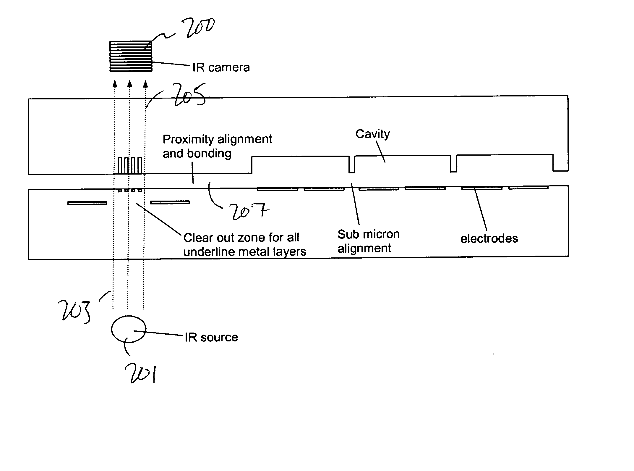
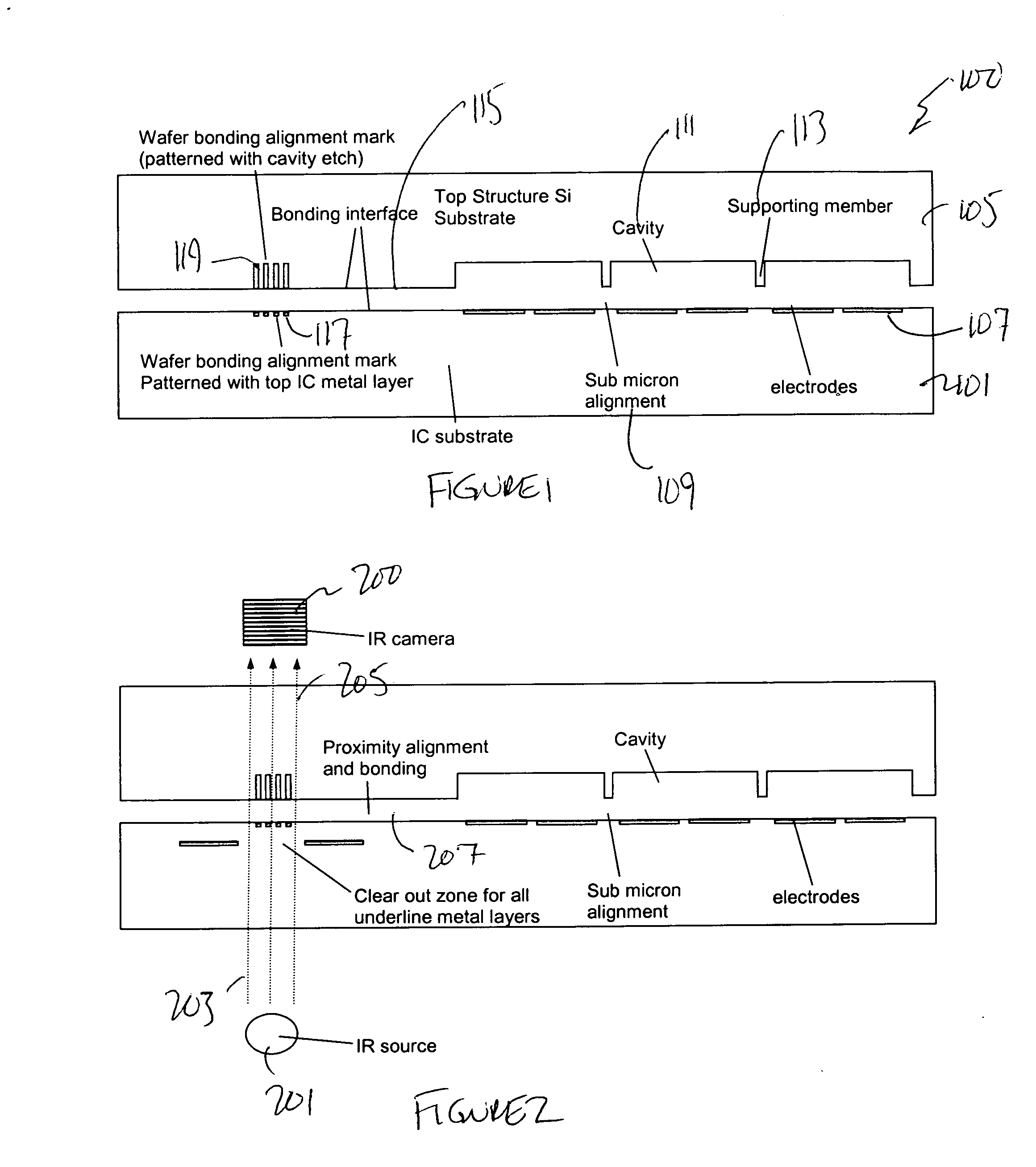
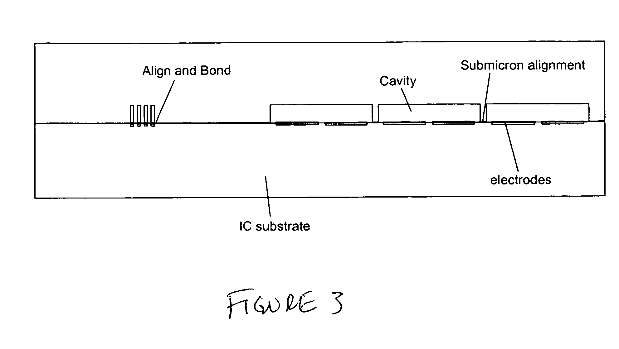
[0012] According to the present invention, techniques for bonding substrates are provided. More particularly, the invention includes a method and structure for bonding substrates together using alignment marks. Merely by way of example, the invention has been applied to integrating a mechanical based structure with an integrated circuit chip. But it would be recognized that the invention has a much broader range of applicability.

[0013] A method for bonding a pair of substrates together according to an embodiment of the present invention may be outlined as follows: [0014] 1. Provide a first substrate comprising a first surface and a plurality of first chips including integrated circuit devices thereon, whereupon the first substrate includes a first alignment mark on the first substrate and a second alignment mark on the first substrate; [0015] 2. Provide a second substrate comprising a silicon bearing material and second surface including a plurality of second chips including a plur...


PUM

PropertyMeasurementUnit
distanceaaaaaaaaaa
widthaaaaaaaaaa
electromagnetic radiationaaaaaaaaaa

Abstract

A method for bonding substrates together. The method includes providing a first substrate comprising a first surface. The first substrate comprises a plurality of first chips thereon. Each of the chips has integrated circuit devices. The first substrate includes a first alignment mark on the first substrate and a second alignment mark on the first substrate. The method also includes providing a second substrate comprising a silicon bearing material and second surface. The second substrate comprising a plurality of second chips thereon. Each of the chips comprises a plurality of mechanical structures. The second substrate has a first silicon based pattern on the second substrate and a second silicon based pattern on the second substrate. The method includes moving the first alignment mark of the first substrate to the first silicon based pattern on the second substrate and aligning the second alignment mark of the first substrate to the second silicon based pattern on the second substrate. A portion of at least one of the first substrate or the second substrate is illuminated with electromagnetic radiation. The method includes detecting a portion of the electromagnetic radiation and using the detected portion of the electromagnetic radiation to align the first substrate with the second substrate. The method also includes coupling the first substrate with the second substrate by contacting the first surface with the second surface and bonding the first surface with the second surface.

Description

BACKGROUND OF THE INVENTION [0001] The present invention relates generally to bonding techniques. More particularly, the invention includes a method and structure for bonding substrates together using alignment marks. Merely by way of example, the invention has been applied to integrating a mechanical based structure with an integrated circuit chip. But it would be recognized that the invention has a much broader range of applicability. [0002] Visual display technologies have rapidly developed over the years. Most particularly, electronic displays for outputting television shows, streaming video, and the like. From the early days, cathode ray tube technology, commonly called CRTs, outputted selected pixel elements onto a glass screen in conventional television sets. These television sets originally output black and white moving pictures. Color television sets soon replaced most if not all black and white television units. Although very successful, CRTs were often bulky, difficult to...

Claims


Application Information

Patent Timeline
Patent Type & Authority Applications(United States)
IPC IPC(8): B81C3/00H01L21/18H01L21/30H01L21/46H01L21/76H01L29/76H01L29/94H01L31/062H01L31/113H01L31/119
CPCH01L21/187B81C2203/051B81C3/004
Inventor YANG, XIAO CHARLES
Owner MIRADIA INC
Why Eureka
Try Eureka