Image-correction-amount detecting device, circuit for driving electro-optical device, electro-optical device, and electronic apparatus

a technology of image correction and detecting device, which is applied in the direction of instruments, computing, electric digital data processing, etc., can solve the problems of significant deformation of image quality, pixel electrode affected by the potential of source line, and display image burn-in phenomenon, so as to reduce the deterioration of display quality, minimize the difference between luminance, and reduce the luminance difference

Inactive Publication Date: 2005-11-24
SEIKO EPSON CORP
View PDF3 Cites 22 Cited by
  • Summary
  • Abstract
  • Description
  • Claims
  • Application Information

AI Technical Summary

Benefits of technology

[0018] An advantage of the invention is that it provides an image-correction-amount detecting device which can calculate the image correction amount of image signal for obtaining an electro-optical device that reduces the deterioration of display quality caused by burn-in or flicker.
[0019] An image-correction-amount detecting device according to an aspect of the invention includes: an image signal generation unit that generates and supplies image signals having inverted polarities to a display section in which pixels are formed so as to correspond to intersections of a plurality of scanning lines and a plurality of source lines which are arranged in a matrix and which performs pixel display by allowing an image signal supplied to a source line to be applied to a pixel electrode of each pixel via switching elements, the image signal being supplied to the source line by turning on a switching element disposed in the pixel with the scanning signal supplied to the scanning line; a luminance detecting unit that detects the luminance of each pixel position of an image displayed by the display section; and a correction value calculation unit that, while changing the reference voltage which is set in the display section, calculates the difference of the luminances between a positive polarity image signal and a negative polarity image signal in each pixel position, calculates the distribution of reference voltages in the display section which applies the minimum luminance difference, and outputs an image correction amount to obtain the optimal reference voltage that matches the effective value of the positive polarity image signal with the effective value of the negative polarity image signal.
[0020] According to this configuration, the image signal generation unit generates the image signals with the inverted polarities to supply to the display section. The luminance detecting unit detects the luminance for each pixel position of the image which is displayed by the display section. The correction value calculation unit calculates the luminance difference between the positive polarity image signal and the negative polarity image signal for each pixel position, while changing the reference voltage which is set in the display section. By changing a reference voltage, it is possible to match the effective values of the positive polarity image signal and the negative polarity image signal which are supplied to the display section. When the effective values matches with each other, the luminance difference decreases. In other word, a reference voltage at which the luminance difference decreases is a voltage of which a direct current of the image signal supplied to the display section is made 0. The correction value calculation section calculates the distribution of reference voltages in the display section, corresponding to the minimum luminance difference, and output the image correction amount to obtain the optimal reference voltage which matches the effective value of the positive polarity image signal with the effective value of the negative polarity image signal. By using the image correction amount, the direct current of image signal supplied to the display section is controlled, which makes it possible to perform a high-quality image display which does not cause any burn-in or flicker.
[0021] In addition, the image correction amount is a value which is obtained by calculating the difference between a set reference voltage set in another display section having the same configuration as the display section and a reference voltage corresponding the minimum luminance difference, for every pixel.
[0022] According to this configuration, by using the image correction amount which minimizes the difference between the luminance of positive polarity image signal and the luminance of negative polarity image signal, it is possible to perform a high-quality image display which does not cause any burn-in or flicker.
[0023] In addition, the luminance detecting unit detects the luminance for a portion of pixel positions of the image and the correction value calculating unit interpolates the luminance detected by the luminance detecting unit to obtain the luminance value for all pixel positions of the image.

Problems solved by technology

However, direct current components of applied signals cause the liquid crystal display device to be contaminated due to impurities within liquid crystal cells or cause liquid crystal components to break down, and cause a burn-in phenomenon of the display image to occur.
However, the pixel electrode is affected by the potential of the source line due to the charge leakage and the coupling capacitance even when the TFT is in an off state.
Due to the potential variation of the voltage applied to the pixel, the display within the screen is not uniform, and the image quality is significantly degraded in the intermediate gray-scale region.
As a result, an optical leakage current occurs, which flows toward the gate of the TFT element.
However, a center portion of an opening region and the surrounding portion have a different amount of optical leakage from each other: the amount of optical leakage increases towards the center of the screen.
As a result, regardless of the alternative current driving, a direct current component is applied to the liquid crystal capacitance, which causes the burn-in phenomenon to occur and causes flicker to occur at the time of positive polarity writing and the negative polarity writing so that the display quality becomes significantly degraded.

Method used


Image

  • Image-correction-amount detecting device, circuit for driving electro-optical device, electro-optical device, and electronic apparatus
  • Image-correction-amount detecting device, circuit for driving electro-optical device, electro-optical device, and electronic apparatus
  • Image-correction-amount detecting device, circuit for driving electro-optical device, electro-optical device, and electronic apparatus

Examples


embodiments

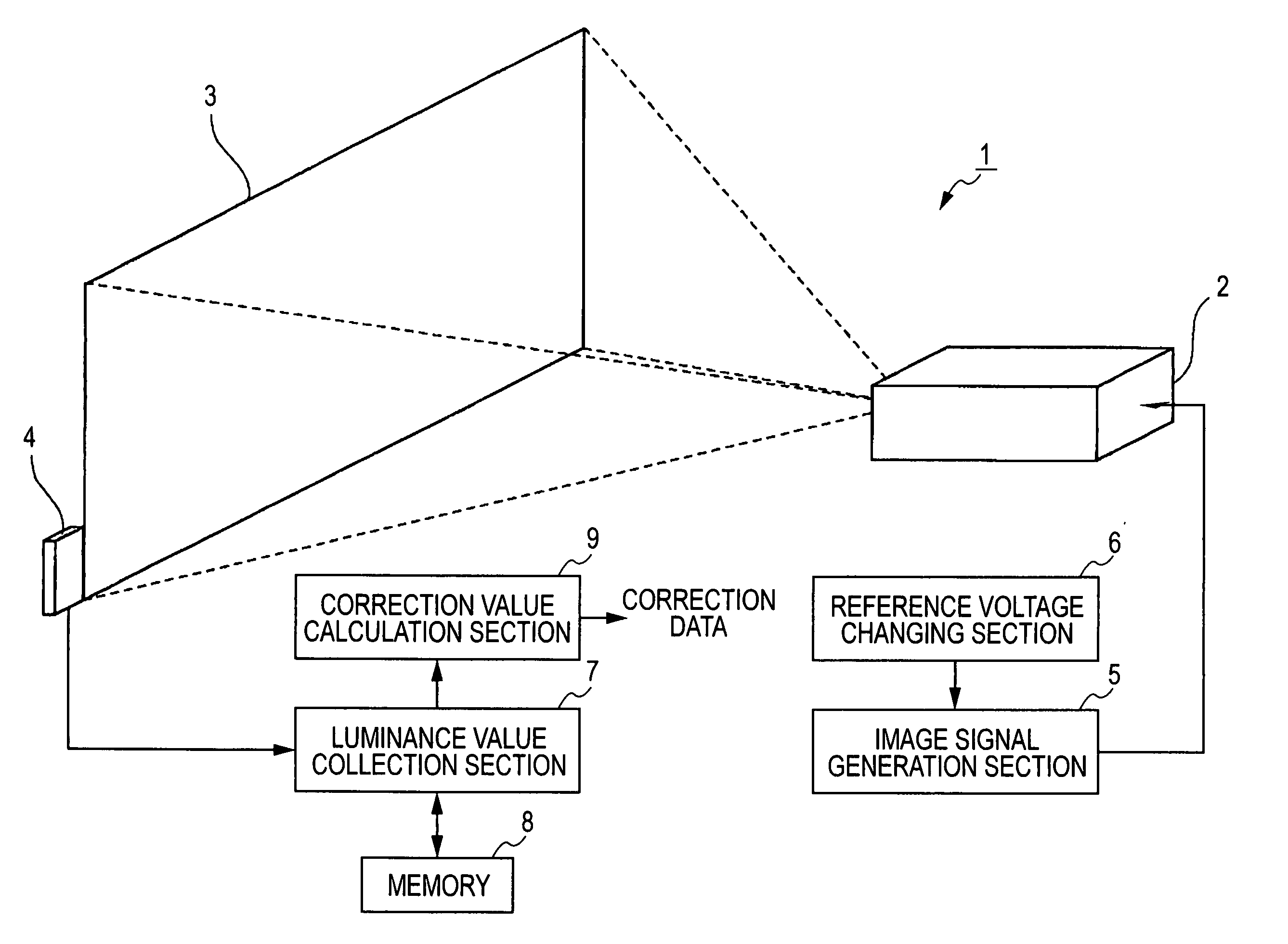
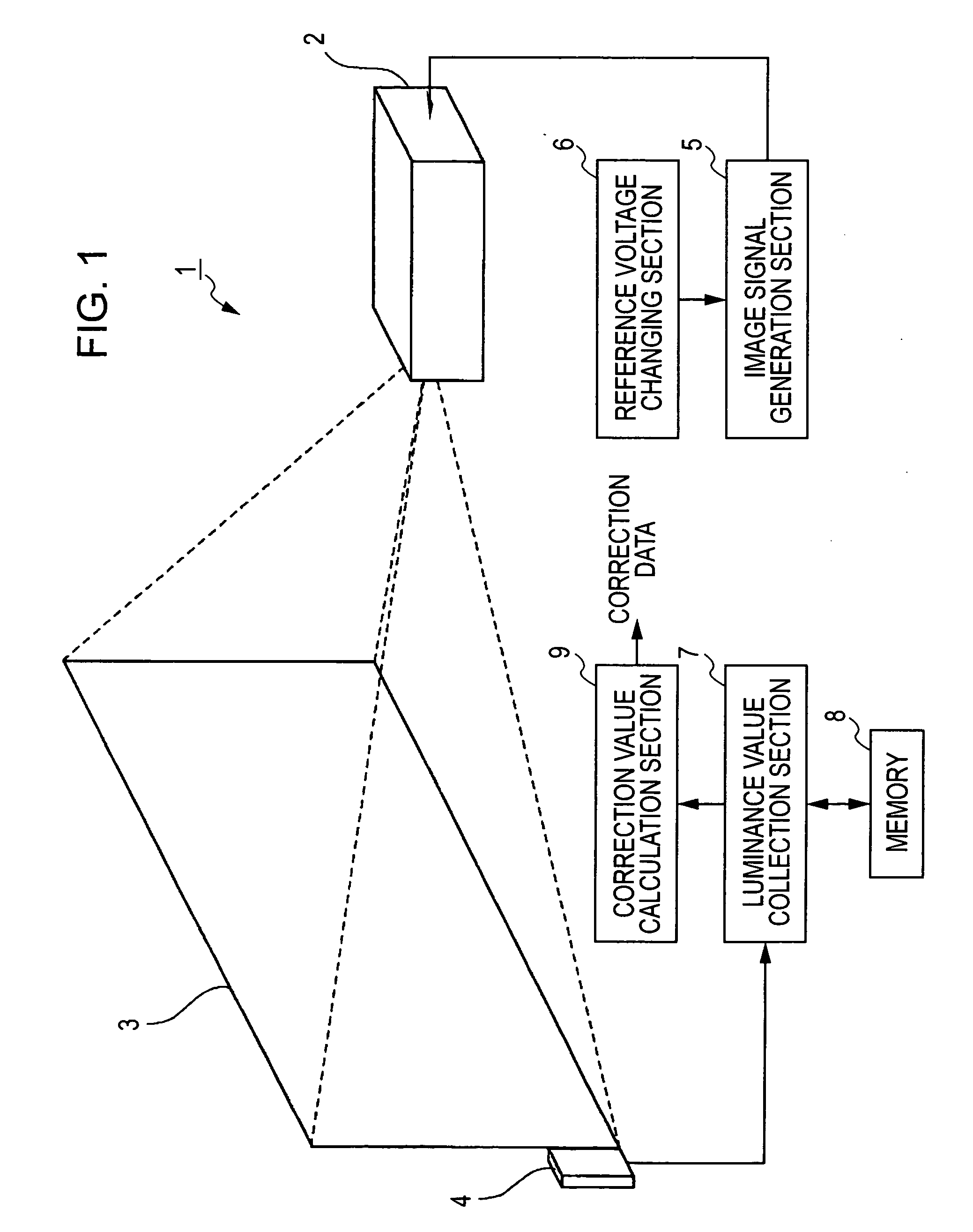
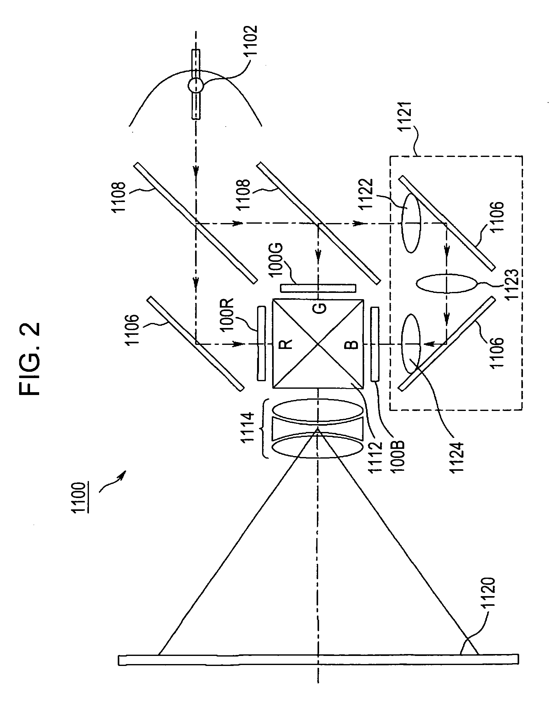
[0046] First, a configuration of an optical system of the projector, which uses the image correction amount calculated by the embodiment, will be schematically described with reference to FIG. 2.

[0047] Referring to FIG. 2, a lamp unit 1102 composed of a white light source such as a halogen lamp is disposed within a projector 1100. Projection light emitted from the lamp unit 1102 is separated into three primary colors of red (R), green (G), and blue (B) by three internal mirrors 1106 and two internal dichroic mirrors 1108; the separated light is then guided to liquid crystal panels100R, 100G, and 100B corresponding to the respective primary colors.

[0048] In this case, image signals of the R, G, and B colors processed by a processing circuit 300 to be described later are supplied to the liquid crystal panels 100R, 100B, and 100G, respectively. Accordingly, the liquid crystal panels 100R, 100B, and 100G serve as optical modulators for generating the images of the primary colors of R,...


PUM


Abstract

An image-correction-amount detecting device includes an image signal generation unit, a luminance detecting unit, and a correction value calculation unit. The image signal generation unit generates and supplies image signals having inverted polarities to a display section in which pixels are formed so as to correspond to intersections of a plurality of scanning lines and a plurality of source lines which are arranged in a matrix and which performs pixel display by allowing an image signal supplied to a source line to be applied to a pixel electrode of each pixel via switching elements, the image signal being supplied to the source line by turning on a switching element disposed in the pixel with the scanning signal supplied to the scanning line. The luminance detecting unit detects the luminance of each pixel position of an image displayed by the display section. While changing the reference voltage which is set in the display section, the correction value calculation unit calculates the difference of the luminance between a positive polarity image signal and a negative polarity image signal in each pixel position, calculates the distribution of reference voltages in the display section which applies the minimum luminance difference, and outputs an image correction amount to obtain the optimal reference voltage that matches the effective value of the positive polarity image signal with the effective value of the negative polarity image signal.

Description

BACKGROUND OF THE INVENTION [0001] 1. Technical Field [0002] The present invention relates to an electro-optical device in which flicker or the like can be reduced over the entire display region, a circuit for driving the same, and an electronic apparatus. [0003] 2. Related Art [0004] Electro-optical devices, for example, such as liquid crystal display devices using liquid crystal as an electro-optical material are widely used, as display devices replacing cathode ray tubes (CRTs), for display units or liquid crystal TVs in, for example, various information processing apparatuses. [0005] Such a liquid crystal display device includes, for example, pixel electrodes arranged in a matrix, an element substrate on which switching elements such as thin film transistors (TFTs) connected to the pixel electrodes are disposed, a counter substrate on which counter electrodes corresponding to the pixel electrodes are disposed, and liquid crystal as the electro-optical material filled between the...

Claims


Application Information

Patent Timeline
Patent Type & Authority Applications(United States)
IPC IPC(8): G09G3/36
CPCG09G3/3614G09G3/3648G09G3/3655G09G2310/0297G09G2360/16G09G2320/0233G09G2320/0247G09G2360/147G09G2320/0219G09G3/20G09G3/36
Inventor AOKI, TORU
Owner SEIKO EPSON CORP
Why Eureka
Try Eureka