

Wired circuit board
a circuit board and wire technology, applied in the field of wired circuit boards, can solve problems such as erroneous examination determination, and achieve the effect of improving accuracy
- Summary
- Abstract
- Description
- Claims
- Application Information
AI Technical Summary
Benefits of technology
Problems solved by technology
Method used
Image

Examples
example 1
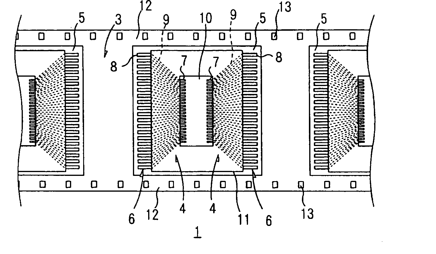
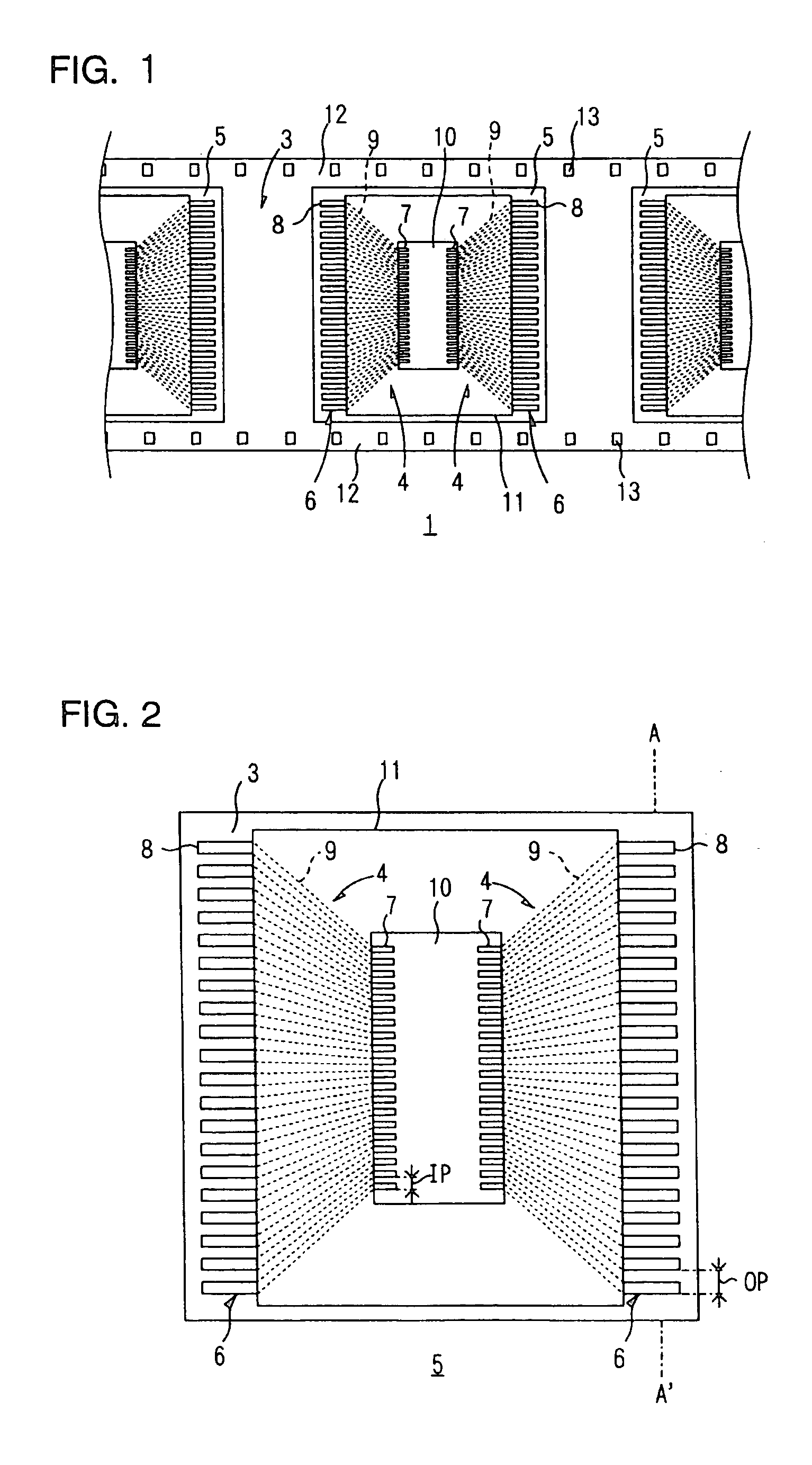
[0071] A metal supporting layer of a stainless foil having a degree of surface brilliancy of 200% (SUS304 of 20 μm thick and 250 mm wide) was prepared, first (Cf. FIG. 4(a)). Then, solution of polyamic acid resin was coated over the metal supporting layer and then was dried. Thereafter, it was cured by heating, to form an insulating layer of polyimide resin having thickness of 25 μm (Cf. FIG. 4(b)). Sequentially, a thin chromium film having thickness of 300 Å and a thin copper film having thickness of 2,000 Å were sequentially formed on the insulating layer by sputtering, to form a seed film (Cf FIG. 4(c)).
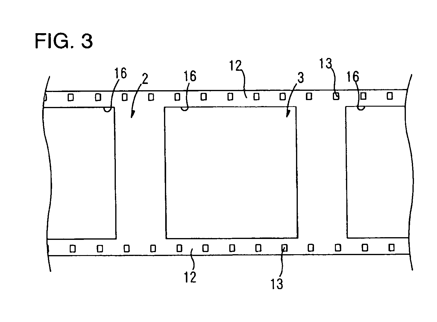
[0072] Thereafter, a number of sprocket holes were bored by punching, to extend through the metal supporting layer, the insulating layer, and the seed film in the thickness direction thereof (Cf. FIG. 4(d)). Then, a plating resist having a predetermined pattern was formed on a surface of the seed film and another plating resist was formed on the entire surface of the metal suppor...
example 2
[0080] Except that a stainless foil having the degree of surface brilliancy of 450% was used, the same operations as those of Example 1 were performed to produce the TAB tape carrier. It was confirmed by the subsequent continuity inspection that the examination result that no erroneous determination was presented as was obtained by the examination of the TAB tape carrier based on the pattern design of the conductor pattern by the light reflection test was correct.
[0081] The haze value of the insulating layer of the TAB tape carrier thus produced was 20%. When an IC chip was mounted on the TAB tape carrier obtained in the same manner as in Example 1, the IC chip was mounted at the correct position.
PUM
| Property | Measurement | Unit |
|---|---|---|
| haze | aaaaa | aaaaa |
| width | aaaaa | aaaaa |
| width | aaaaa | aaaaa |
Abstract
Description
Claims
Application Information