Method of manufacturing circuit device

a manufacturing method and circuit technology, applied in the field of manufacturing circuit devices, can solve the problems of increasing manufacturing costs and inhibiting the miniaturization of the entire device, and achieve the effect of reducing manufacturing costs and high precision

Inactive Publication Date: 2005-12-01
SANYO ELECTRIC CO LTD
View PDF2 Cites 9 Cited by
  • Summary
  • Abstract
  • Description
  • Claims
  • Application Information

AI Technical Summary

Benefits of technology

[0011] According to the circuit device-manufacturing method of the present invention, the conductive pattern can be partially exposed from the coating resin with high precision without using an exposure mask. Specifically, the protruding portions can be exposed by coating with the coating resin the conductive pattern in which the protruding portions protruding above other regions, and then uniformly removing the coating resin from the surface thereof. Accordingly, the conductive pattern can be partially exposed without performing a lithography step as in the known example. Thus, a pattern can be designed with no consideration given to errors occurring in the lithography step. Consequently, the miniaturization of the entire circuit device can be realized. Furthermore, the elimination of the lithography step makes it possible to provide a circuit device-manufacturing method in which the manufacturing cost is reduced.

Problems solved by technology

This inhibits the miniaturization of the entire device.
Further, the lithography step itself performed for partially removing the coating resin 109 increases the manufacturing cost.

Method used


Image

  • Method of manufacturing circuit device
  • Method of manufacturing circuit device
  • Method of manufacturing circuit device

Examples


Embodiment Construction

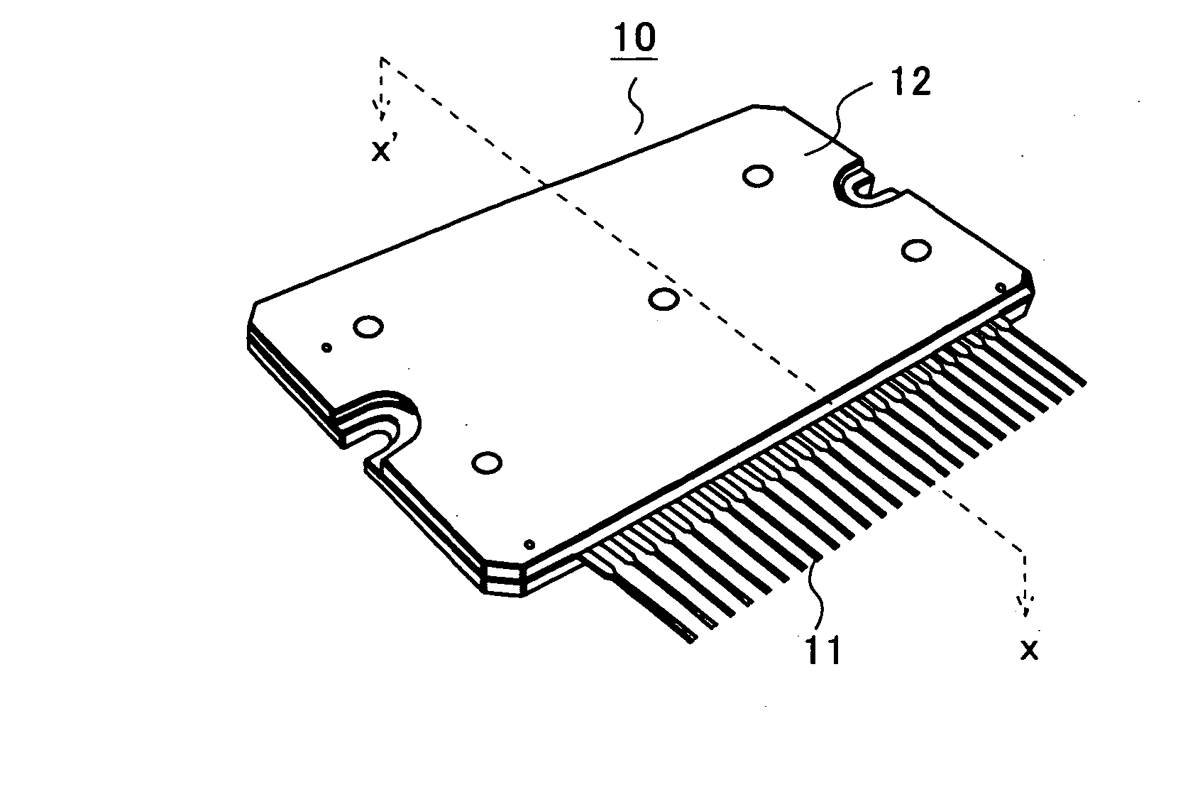
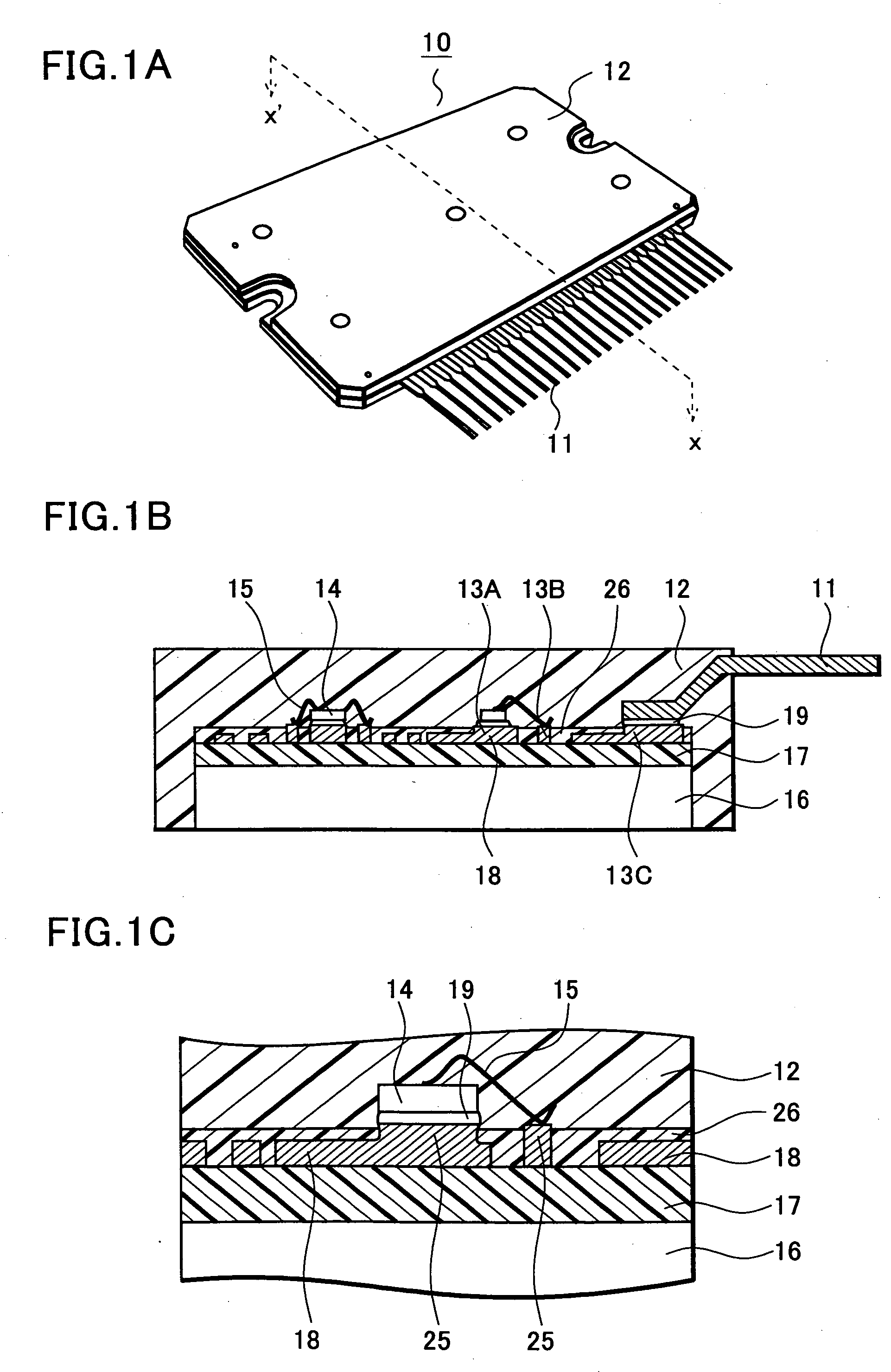
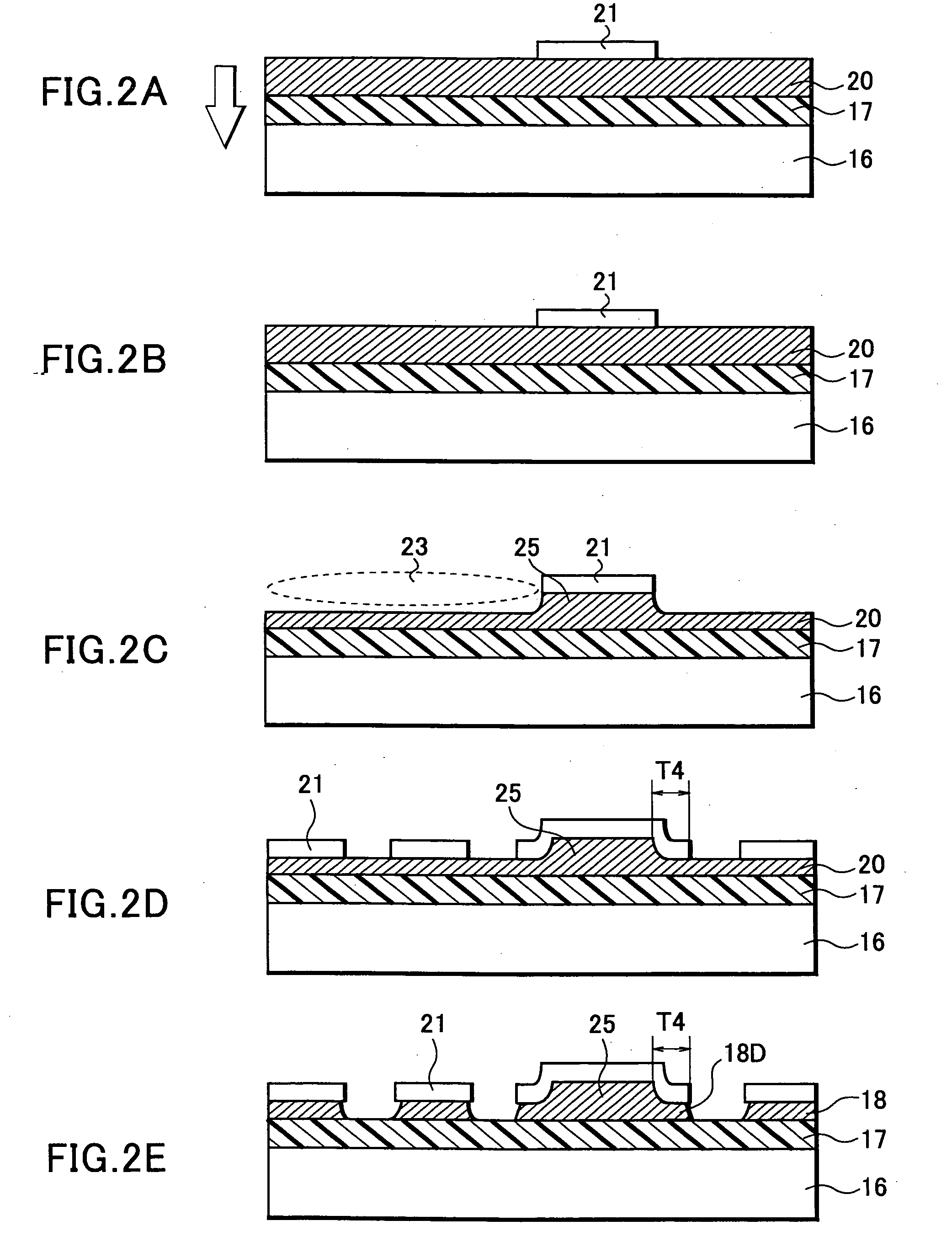
[0019] The constitution of a hybrid integrated circuit device 10 as one example of a circuit device of the present invention will be described with reference to FIGS. 1A to 1C. FIG. 1A is a perspective view of the hybrid integrated circuit device 10. FIG. 1B is a cross-sectional view taken along the X-X′ line of FIG. 1A. FIG. 1C is an enlarged cross-sectional view of a region in which protruding portions 25 are formed in a conductive pattern 18.

[0020] The hybrid integrated circuit device 10 of this embodiment includes a circuit substrate 16 having an insulating layer 17 formed on the front surface thereof, and the conductive pattern 18 formed on the surface of the insulating layer 17. Further, the conductive pattern 18 is coated with coating resin 26, except for electrical connection regions. Furthermore, circuit elements 14 electrically connected to the conductive pattern 18 are sealed with sealing resin 12. Details of the hybrid integrated circuit device 10 having the above-descr...


PUM

PropertyMeasurementUnit
thicknessaaaaaaaaaa
thicknessaaaaaaaaaa
conductiveaaaaaaaaaa

Abstract

In a method of manufacturing a circuit device of the present invention, protruding portions protruding upward are formed in part of a conductive pattern formed on the front surface of a circuit substrate. Next, the front surface of the circuit substrate including the protruding portions is coated with coating resin. Subsequently, the coating resin is etched so that the top surfaces of the protruding portions are exposed. Then, the fixation and electrical connection of circuit elements are performed. Finally, an electric circuit formed on the front surface is sealed, whereby a hybrid integrated circuit device is completed.

Description

BACKGROUND OF THE INVENTION [0001] Priority is claimed to Japanese Patent Application Number JP2004-162655 filed on May 31, 2004, the disclosure of which is incorporated herein by reference in its entirety. [0002] 1. Field of the Invention [0003] The present invention relates to a method of manufacturing a circuit device. In particular, the present invention relates to a method of manufacturing a circuit device having coating resin which coats a conductive pattern. [0004] 2. Description of the Related Art [0005] The constitution of a known hybrid integrated circuit device will be described with reference to FIGS. 7A and 7B. This technology is described for instance in Japanese Patent Publication No. Hei 6(1994)-177295 (page 4, FIG. 1). FIG. 7A is a perspective view of the hybrid integrated circuit device 100, and FIG. 7B is a cross-sectional view taken along the X-X′ line of FIG. 7A. [0006] The known hybrid integrated circuit device 100 has the following constitution. The hybrid int...

Claims


Application Information

Patent Timeline
Patent Type & Authority Applications(United States)
IPC IPC(8): B44C1/22H01B13/00H05K3/34H01L21/28H01L21/48H01L21/98H01L23/12H05K1/02H05K1/05H05K3/00H05K3/28H05K3/40
CPCH01L21/4821H01L2924/01005H01L24/97H01L25/50H01L2221/68377H01L2224/48091H01L2224/73265H01L2224/97H01L2924/01013H01L2924/01029H01L2924/01033H01L2924/01078H01L2924/01082H01L2924/13055H01L2924/14H01L2924/19041H05K1/056H05K3/28H05K3/284H05K3/4007H05K2203/0369H05K2203/1476H01L21/4871H01L2924/01006H01L2924/1305H01L2924/1301H01L2924/13091H01L2924/07802H01L2924/10253H01L2924/12041H01L2924/00014H01L2224/92247H01L2224/85H01L2224/83H01L2924/00H01L2924/351H01L2924/181H01L2924/00012H01L23/40
Inventor TAKAKUSAKI, SADAMICHINEZU, MOTOICHIKUSABE, TAKAYA
Owner SANYO ELECTRIC CO LTD
Why Eureka
Try Eureka