Injection molded continuously solidified solder method and apparatus

a technology of injection molding and solidification solder, which is applied in the direction of welding/cutting media/materials, manufacturing tools, and solventing apparatus, etc., can solve the problems of inability to meet the requirements of process operation, inability to accurately deposition solder, and high cost of process and maintenance steps. achieve the effect of accurate deposition of solder

Inactive Publication Date: 2005-12-01
BELANGER LUC +12
View PDF17 Cites 70 Cited by
  • Summary
  • Abstract
  • Description
  • Claims
  • Application Information

AI Technical Summary

Benefits of technology

[0010] It is therefore an aspect of the present invention to provide a method and an apparatus for the accurate deposition of solder in cavities in a substrate, including complete filling of the cavities.
[0011] It is another aspect of this invention to provide a method and apparatus which fills such cavities without leaving debris that must be removed in a separate process.
[0012] It is yet another aspect of this invention to provide a substrate that has cavities in a surface of the substrate that have been filled with solder which has been solidified so as to accurately and completely fill the cavities.
[0013] A satisfactory solution to all these problems is to solidify the solder before it exists the trailing edge of the scanning IMS fill head. This solves the first problem in that solidified solder in cavities can no longer ball-up, regardless of how low oxygen levels are. It will also solve the second problem by allowing far lower oxygen levels to be used, which will all but eliminate excessive oxidation from contaminating either the mold plate surface or the head. The third problem of fill non-uniformities due to incomplete fill and solder bridging is also eliminated due to a) a new narrow slot geometry assuring optimized fill and b) solidification taking place while the constraining surface of the scanning head is still over the filled cavities, thus assuring fill levels coplanar with the top surface of the cavities.
[0014] This novel solution has the advantage over the “shaving” solution in that 1) no extra processing steps are required and 2) no mechanical damage can occur to the mold plate. Additionally, this solution allows the use of polyimide-on-glass mold plates in the same manner as etched glass mold plates, since no mechanical “shaving” is required that would quickly damage the softer polyimide layer. For these and other reasons, the present invention is the ideal solution to making the new IMS process truly manufacturable.

Problems solved by technology

These problems having to do with molten solder exiting behind the scanning head.
Referring to FIG. 2, the first problem is that at oxygen levels much lower than 1-2%, the molten solder in cavities exiting behind the fill head will actually ball-up, meaning the solder volume changes in shape from the hemispherical cavity to a full sphere 36 with reduced surface area in contact with the cavity walls.
On solidification, these solder balls are thus easily dislocated from the cavities before the transfer step, making the process bump yield unacceptable.
Thus, this second problem adds costly process and maintenance steps to IMS wafer bump manufacturing, imperiling the low-cost attribute of the process.
The third problem is associated with surface tension induced fill non-uniformities typically caused by the trailing edge 39 of the contact plate 24.
Solder bridging 40 is removed before the mold plate is transferred to the wafer, but this adds process costs and steps.
This solves problems two and three, but adds other problems, namely extra process steps and mechanical damage to mold plates.
If the mold plates are glass, this shaving step reduces mold plate lifetimes. If the mold plates are glass with coated polyimide containing the cavities, then this is not possible since it will damage the softer polyimide material.
Thus, all these solutions are unsatisfactory from a manufacturing standpoint.

Method used


Image

  • Injection molded continuously solidified solder method and apparatus
  • Injection molded continuously solidified solder method and apparatus
  • Injection molded continuously solidified solder method and apparatus

Examples


Embodiment Construction

[0046] Variations described for the present invention can be realized in any combination desirable for each particular application. Thus particular limitations, and / or embodiment enhancements described herein, which may have particular advantages to the particular application need not be used for all applications. Also, it should be realized that not all limitations need be implemented in methods, systems and / or apparatus including one or more concepts of the present invention.

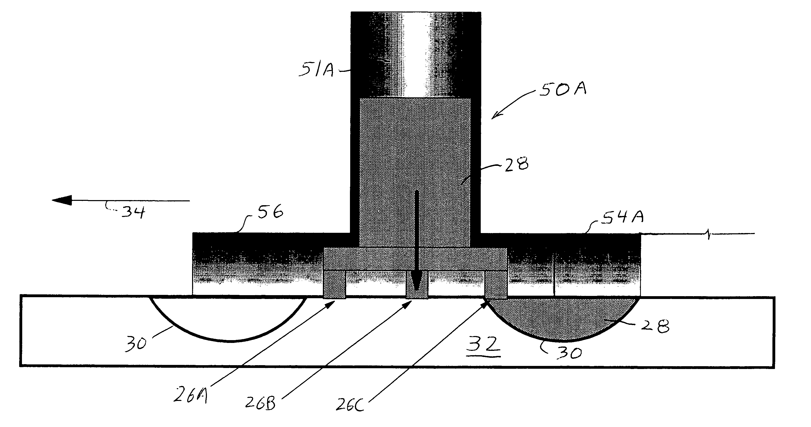
[0047] Referring to FIG. 5, a key feature of this invention is an IMS head 50 with a generally longer die or contact plate 52 which includes a cooling zone 54 after the hot solder injection zone 56. The solder 28, from reservoir 51, solidifies across each cavity in the mold plate 32 in the direction of the scan, as represented by arrow 34, and by solidified solder 28A and still molten solder 28B, with the solidification taking place as molten solder comes into contact with cooling zone 54 of contact plate 52....


PUM

PropertyMeasurementUnit
widthaaaaaaaaaa
widthaaaaaaaaaa
widthaaaaaaaaaa

Abstract

A method and apparatus for forming solder bumps by molten solder deposition into cavity arrays in a substrate immediately followed by solidification of molten solder such that precise replication of cavity volumes is consistently achieved in formed solder bump arrays. Various solder filling problems, such as those caused by surface tension and oxidation effects, are overcome by a combination of narrow molten Solder dispense slots and solidification of dispensed molten solder.

Description

FIELD OF THE INVENTION [0001] This invention relates to the field of solder interconnects formed between silicon circuit devices and substrates forming the next layer of electrical interconnect. More specifically, the invention relates to improvements in injection molded solder technologies used to form solder bump interconnections on silicon wafers. BACKGROUND OF THE INVENTION [0002] Injection Molded Soldering (IMS) is a new process with many applications, primarily suited for low-cost solder bumping of semiconductor wafers. It basically involves scanning a head which dispenses molten solder through a linear slot over a mold plate to fill cavities therein with molten solder. After the scan, the solder in the cavities is solidified and then the mold plate is aligned to and placed in contact with a wafer by an appropriate fixture. This assembly is then heated to re-flow and transfer the solder from the mold plate cavities to metallized pads on the wafer. After cooling and separating ...

Claims


Application Information

Patent Timeline
Patent Type & Authority Applications(United States)
IPC IPC(8): B23K3/06B23K31/02H05K3/34
CPCB23K3/0623H05K3/3457H05K2203/1121H05K2203/0126H05K2203/0338H05K2203/0113
Inventor BELANGER, LUCBROUILLETTE, GUYBUCHWALTER, STEPHEN L.GRUBER, PETER A.KIMURA, HIDEOLANDREVILLE, JEAN-LUCMANURER, FREDERICMONTMINY, MARCOBERSON, VALERIESHIH, DA-YUANST-ONGE, STEPHANETURGEON, MICHELYAMADA, TAKESHI
Owner BELANGER LUC
Why Eureka
Try Eureka