

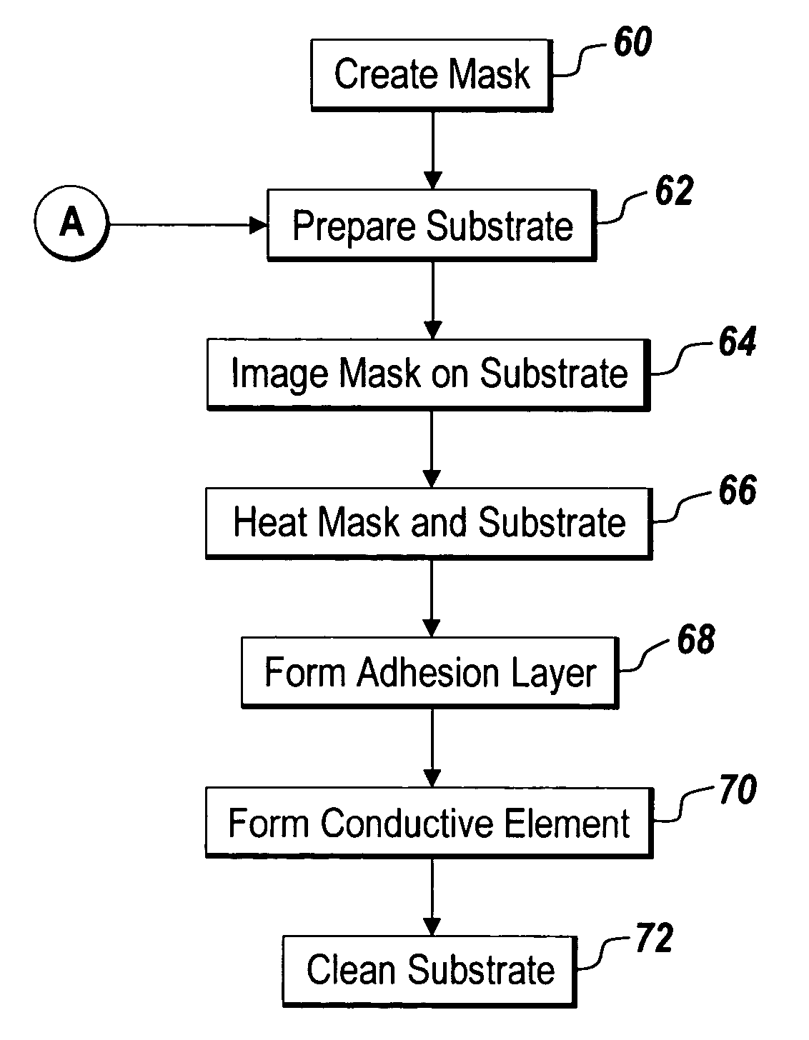
Method for pattern metalization of substrates
a technology of pattern metalization and substrate, applied in the direction of electrographic process, non-linear optics, instruments, etc., can solve the problems of time-consuming and costly conventional photolithography patterning techniques, cost and time associated with conventional photolithography is the development and fabrication of masks, and the total cost of use, so as to improve the adhesion of the first conductive layer
- Summary
- Abstract
- Description
- Claims
- Application Information
AI Technical Summary
Benefits of technology
Problems solved by technology
Method used
Image

Examples
example i
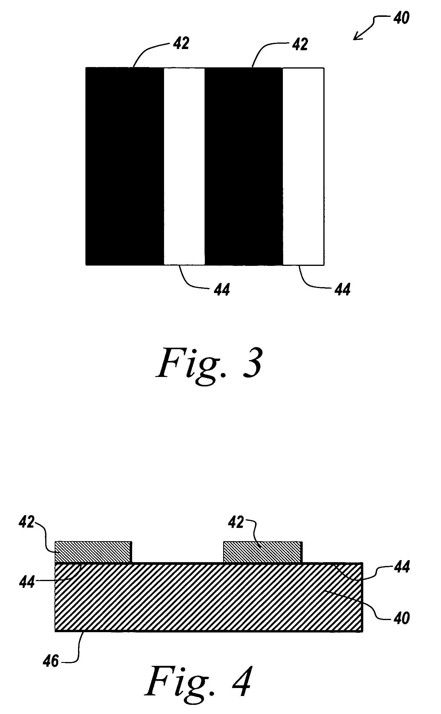
[0083] A conductive pattern is fabricated on substrate 40 according the teachings of the present invention. Substrate 40 is polyimide (Kapton® E) film having thickness of about 51 μm. The polyimide film is removably attached to an 8½×11 sheet of paper (stiffener) by means of mounting tape. A negative electrophotographic imaging compound pattern is imaged on the polyimide film attached to the sheet of paper as stiffener using a laser printer, for example a Hewlett Packard LaserJet 5P, available from Hewlett Packard of Palo Alto, Calif. The sheet of paper is removed and the electrophotographic imaging compound and the polyimide film are baked in air for about one minute at a temperature of about 120° C. About a 10 nm thick layer of chromium (Cr) is deposited by Electron-beam evaporation on the polyimide film and the electrophotographic imaging compound under vacuum to form an adhesion layer. A layer of titanium (Ti) follows the layer of Cr. The Ti has a thickness of about 100 nm is de...
example ii
[0084] Using a substrate 40 of polyimide (Kapton® E) film having a thickness of about 51 μm a conductive pattern is fabricated thereon. The polyimide film is temporarily attached to a sheet of 8½×11 paper (stiffener) by means of mounting tape. A negative electrophotographic imaging compound pattern is imaged on the polyimide film using a laser printer for example a Hewlett Packard LaserJet 5P, available from Hewlett Packard of Palo Alto, Calif. The sheet of paper is removed from the polyimide film and the electrophotographic imaging compound and the polyimide film are baked in air for about 1 minute at about 120° C. About a 10 nm thick layer of Ti is deposited by Electron-beam evaporation on the polyimide film and the electrophotographic imaging compound under vacuum to form an adhesion layer. Next, about a 100 nm thick layer of gold (Au) is deposited by Electron-beam evaporation on the layer of Ti under vacuum. The polyimide film with the layers of Ti and Au is rubbed with a foam s...
example iii
[0085] Using an overhead transparency or a piece of polyester film having a thickness of about 5 mil for substrate 40, a conductive pattern is fabricated as shown in FIG. 7. A negative electrophotographic imaging compound pattern is imaged on the transparency / polyester film using a laser printer, for example a Hewlett Packard LaserJet 5P, available from Hewlett Packard of Palo Alto, Calif. No stiffener is used. The electrophotographic imaging compound and transparency / polyester film is baked in air for about one minute at a temperature of about 120° C. Next, a layer of Ti having a thickness of about 10 nm is deposited on electrophotographic imaging compound and transparency / polyester film the by Electron-beam evaporation under vacuum to form an adhesion layer. The layer of Ti is followed by another Electron-beam evaporation process under vacuum to form a layer of Au having a thickness of about 100 nm on the layer of Ti. The transparency / polyester film with the layer of Ti and Au is ...
PUM
| Property | Measurement | Unit |
|---|---|---|
| Adhesion strength | aaaaa | aaaaa |
| Flexibility | aaaaa | aaaaa |
| Electrical conductor | aaaaa | aaaaa |
Abstract
Description
Claims
Application Information