
Eureka
For R&D, Eureka makes reading and utilizing patents & technical documents easy.
Eureka AIR
Designed for self-driven R&D workflows. Generate viable solutions, solve complex R&D challenges, empower your innovation with AI.

Eureka Materials
Designed for material experts only. Revolutionize your material R&D, from search, analyze, to developing new materials.

TechResearch
Generate reliable direction feasibility study reports for your R&D in just a few steps.

TechSeek
Discover and master advanced knowledge NOW. Basics, ideas, possibilities, all at once.

TechMind
As an expert in R&D Theories, TechMind can generates customized viable solutions instantly.

TechRisk
Analyze your overall solution with one click, know your potential R&D risks in advance.

TechMonitor
Get weekly tech updates, stay abreast of the latest tech innovations and key insights.
Surface-emitting type semiconductor laser, and method for manufacturing the same, optical switch, and optical branching ratio variable element
- Summary
- Abstract
- Description
- Claims
- Application Information
AI Technical Summary
Benefits of technology
Problems solved by technology
Method used
Image

Examples
Embodiment Construction
[0103] Preferred embodiments of the present invention are described below with reference to the accompanying drawings.
[0104] 1. Device Structure
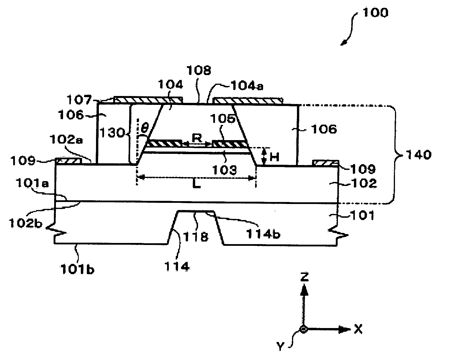
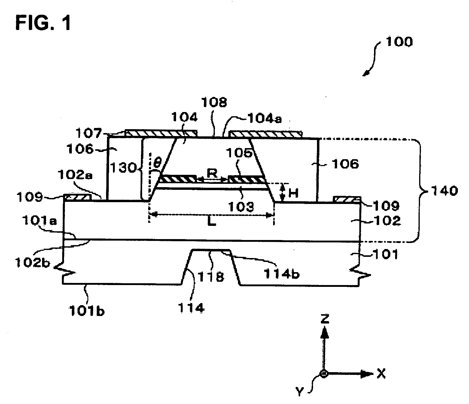
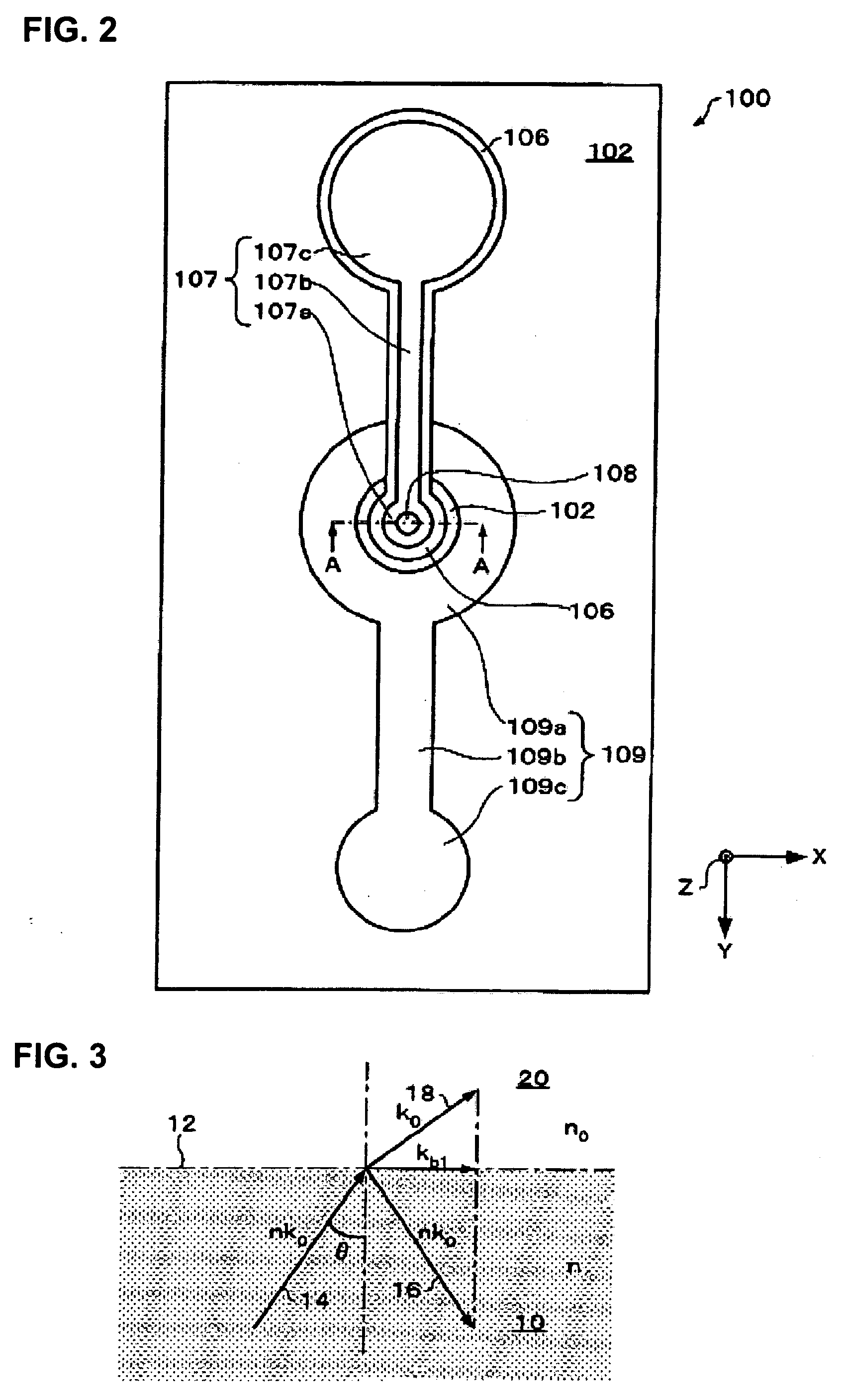
[0105]FIG. 1 is a cross-sectional view schematically showing an optical element 100 in accordance with the present invention, and FIG. 2 is a plan view schematically showing the optical element 100 shown in FIG. 1. FIG. 1 is a cross-sectional view taken along a line A-A of FIG. 2. First, an example in which the optical element 100 is a surface-emitting type semiconductor laser is described. It is noted that the optical element 100 is referred hereunder to as a surface-emitting type semiconductor laser (hereinafter also referred to as a “surface emitting laser”) 100.
[0106] As shown in FIG. 1 and FIG. 2, the surface-emitting laser 100 in accordance with an embodiment of the present invention includes a substrate (a GaAs substrate in the present embodiment) 101, a vertical resonator (hereafter referred to as a “resonator”) 140 formed on the ...
PUM
 Abstract
Description
Claims
Application Information
 - R&D Engineer
- R&D Manager
- IP Professional
- Industry Leading Data Capabilities
- Powerful AI technology
- Patent DNA Extraction
Browse by: Latest US Patents, China's latest patents, Technical Efficacy Thesaurus, Application Domain, Technology Topic, Popular Technical Reports.
© 2024 PatSnap. All rights reserved.Legal|Privacy policy|Modern Slavery Act Transparency Statement|Sitemap|About US| Contact US: help@patsnap.com