Active pixel sensor cell with integrating varactor and method for using such cell

Active Publication Date: 2005-12-08
OMNIVISION TECH INC
View PDF3 Cites 15 Cited by
  • Summary
  • Abstract
  • Description
  • Claims
  • Application Information

AI Technical Summary

Problems solved by technology

One drawback of conventional active pixel sensor cells is that they typically operate poorly under low light conditions.
However, when the exposure period is sufficiently long (e.g., on the order of milliseconds) incident photons cannot accurately be sensed because dark current during the exposure period reduces the photodiode voltage by a

Method used


Image

  • Active pixel sensor cell with integrating varactor and method for using such cell
  • Active pixel sensor cell with integrating varactor and method for using such cell
  • Active pixel sensor cell with integrating varactor and method for using such cell

Examples


Embodiment Construction

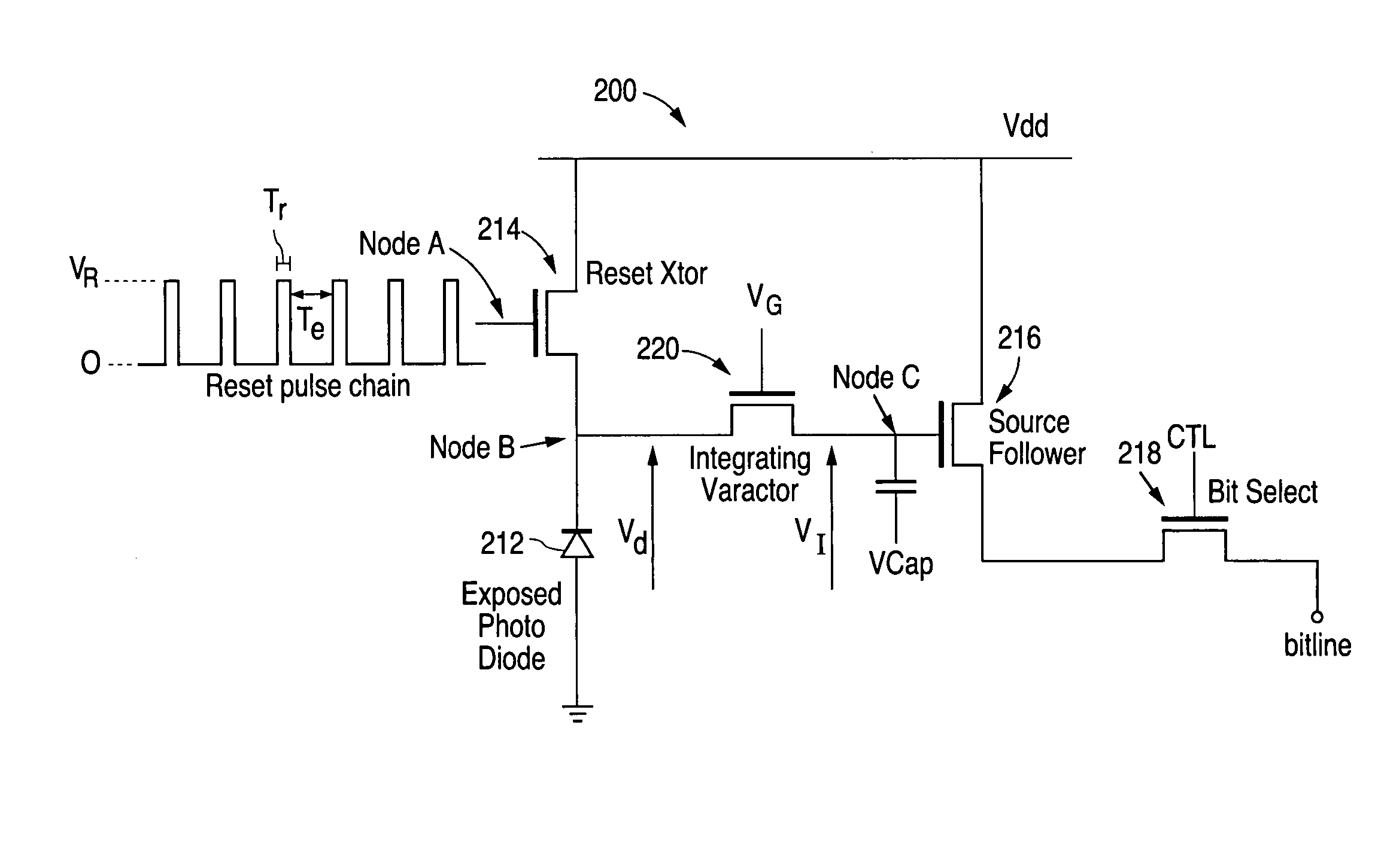
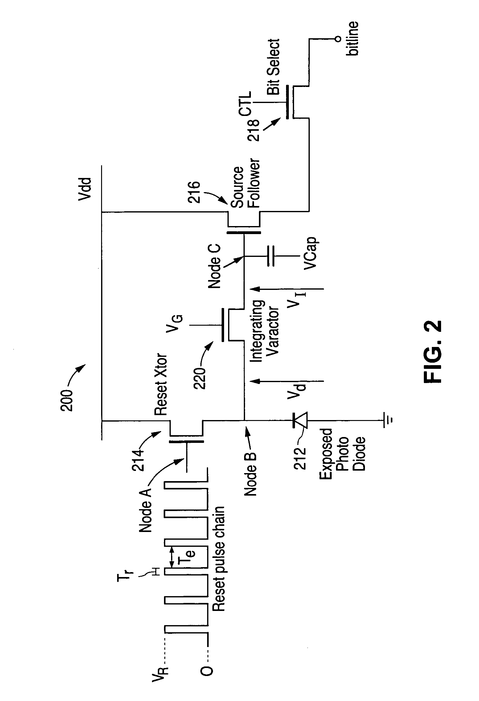
[0021] In a class of embodiments, the invention is an active pixel sensor cell that includes at least one photodiode and reset circuitry and an integrating varactor coupled to the photodiode. The reset circuitry is configured to reset the photodiode multiple times during an exposure interval that includes N subexposure intervals, where 2 N (typically, N is greater than 100) so the photodiode can be reset (during a reset interval) before each of the subexposure intervals. The cell has a first capacitance at a first node of the photodiode, the varactor is coupled between the first node and a storage node, the varactor provides a varactor capacitance at the storage node, and the varactor capacitance is much greater than the first capacitance. The first node is typically a terminal of the photodiode, and another terminal of the photodiode is grounded. During each subexposure interval, a subexposure charge accumulates at the first node as a result of photogeneration in the photodiode. Th...


PUM


Abstract

An active pixel sensor cell including at least one photodiode and reset circuitry and an integrating varactor coupled to the photodiode, a method for reading out such a cell, and an image sensor including an array of such cells. The photodiode can be exposed to photons during an exposure interval to accumulate a sequence of subexposure charges at a first node of the photodiode. Each of the subexposure charges accumulates at the first node during a different subexposure interval of the exposure interval. The photodiode is reset during each of a sequence of reset intervals, each reset interval occurring before a different one of the subexposure intervals. An output signal indicative of an exposure charge accumulated at the storage node during the exposure interval can be asserted from the cell, where the exposure charge is indicative of a sum of all the subexposure charges.

Description

BACKGROUND OF THE INVENTION [0001] 1. Field of the Invention [0002] The present invention pertains to active pixel sensor cells (e.g., MOS active pixel sensor cells that include at least one MOS transistor and at least one photodiode) and to methods of using them. In some embodiments, the invention pertains to active pixel sensor cells that include at least one photodiode and an integrating varactor for each photodiode, and to methods for using such a cell to generate an exposure signal including by charging a capacitance of one such varactor during a sequence of photodiode subexposures (subintervals of an overall photodiode exposure interval). [0003] 2. Description of the Related Art [0004] The expression “MOS device” is used herein as a synonym for an MOS transistor. [0005] The term “varactor” is used herein to denote a semiconductor device in which the electrical characteristic of primary interest is a voltage-dependent capacitance. For example, an NMOS (or PMOS) transistor can b...

Claims


Application Information

Patent Timeline
IPC IPC(8): H01L27/146H04N5/353H04N5/361H04N5/3745
CPCH01L27/14609H04N5/37452H04N5/361H04N5/35572H04N25/587H04N25/63H04N25/771H01L27/146
Inventor HOPPER, PETER J.LINDORFER, PHILIPPPOULTER, MARK W.MIRGORODSKI, YURI
Owner OMNIVISION TECH INC
Why Eureka
Try Eureka