
Optical sensor circuit, method of processing output signal of the same, and electronic apparatus

Active Publication Date: 2005-12-08
138 EAST LCD ADVANCEMENTS LTD
View PDF2 Cites 17 Cited by
  • Summary
  • Abstract
  • Description
  • Claims
  • Application Information

AI Technical Summary

Benefits of technology

[0009] An advantage of the invention is that it provides an optical sensor circuit which can prevent detection precision from deteriorating due to noise or dark current by a light-receiving element itself, a method of processing an output signal of the optical sensor circuit, and an electronic apparatus.
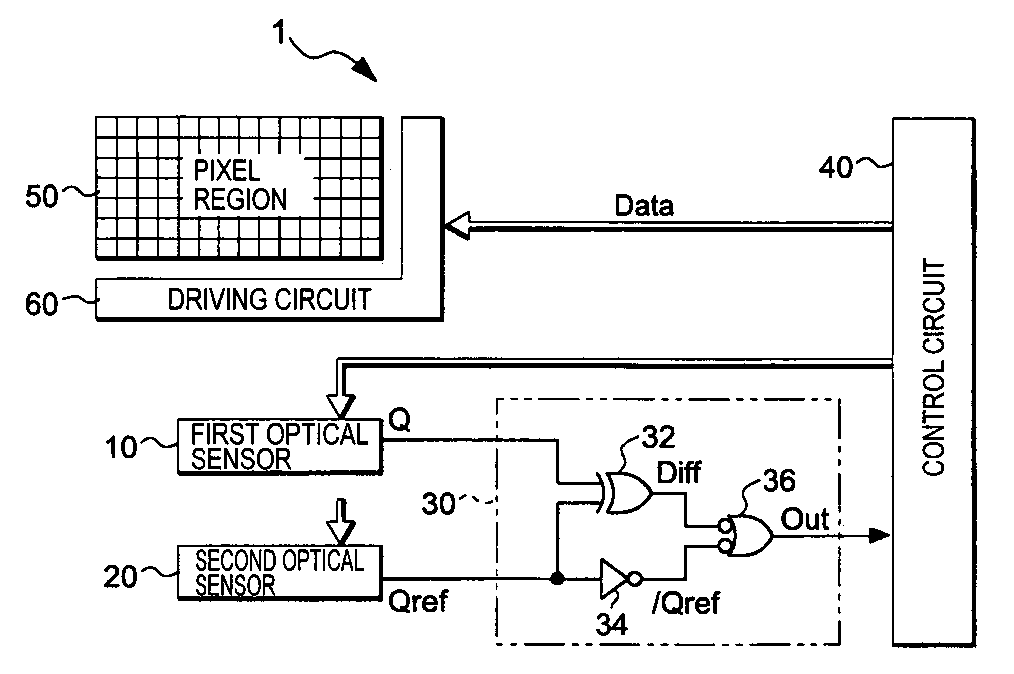
[0010] According to an aspect of the invention, there is an optical sensor circuit including a first optical sensor that outputs a signal according to the amount of received light on an opened light-receiving surface, a second optical sensor that is provided near the first optical sensor and outputs a signal according to the amount of received light on a shielded light-receiving surface, and a difference calculating circuit that calculates a difference between the output signal of the first optical sensor and the output signal of the second optical sensor and outputs the difference. According to this optical sensor circuit, the output signal of the second optical sensor that is provided near the first optical sensor is detected as a reference signal of noise or dark current generated in the first optical sensor. The reference signal is subtracted from the output signal of the first optical sensor and the subtraction result is output as a differential value. For this reason, an influence on the differential value by the noise or the dark current is eliminated and thus degradation in detection precision is prevented.
[0011] In the optical sensor circuit, it is preferable that the first and second optical sensors output logical signals having pulse widths according to the amounts of received light respectively and the difference calculating circuit has an EX-OR circuit that calculates an exclusive logical sum signal of the output signal of the first optical sensor and the output signal of the second optical sensor. According to this configuration, since the difference calculating circuit can be configured with a logical circuit, the configuration can be simplified.
[0012] In addition, in this configuration, since information about the pulse width of the output signal of the second optical sensor is stored in a memory or the like and is read from the memory, the second optical sensor needs to be operated at all times. At this time, the information about the pulse width of the output signal of the second optical sensor may be updated at a constant interval.
[0013] Besides, the invention can be conceptualized as a method of processing of an output signal of the optical sensor circuit, as well as the optical sensor circuit. Furthermore, since an electronic apparatus according to another aspect of the invention has the above-described optical sensor circuit, a display unit can be controlled more correctly by the differential value.

Problems solved by technology

For this reason, when brightness or image quality of a display element is constant irregardless of external light, there is an inconsistency in that, while the display panel can be easily viewed under some conditions, it can hardly be viewed under other conditions.
In this case, however, if the light-receiving element is provided separately from the display panel, a space for mounting the light-receiving element is required extra in the electronic apparatus.
In this technique, the detection precision of light amount is degraded due to the noise mixed into an output line.
However, when the light-receiving element is formed with the same process as that of the thin film transistor for switching the pixel in the display panel, the detection precision of light amount is degraded due to the noise or dark current by the light-receiving element itself.

Method used


Image

  • Optical sensor circuit, method of processing output signal of the same, and electronic apparatus
  • Optical sensor circuit, method of processing output signal of the same, and electronic apparatus
  • Optical sensor circuit, method of processing output signal of the same, and electronic apparatus

Examples


Embodiment Construction

[0021] Hereinafter, an embodiment according to the invention will be described with reference to the drawings.

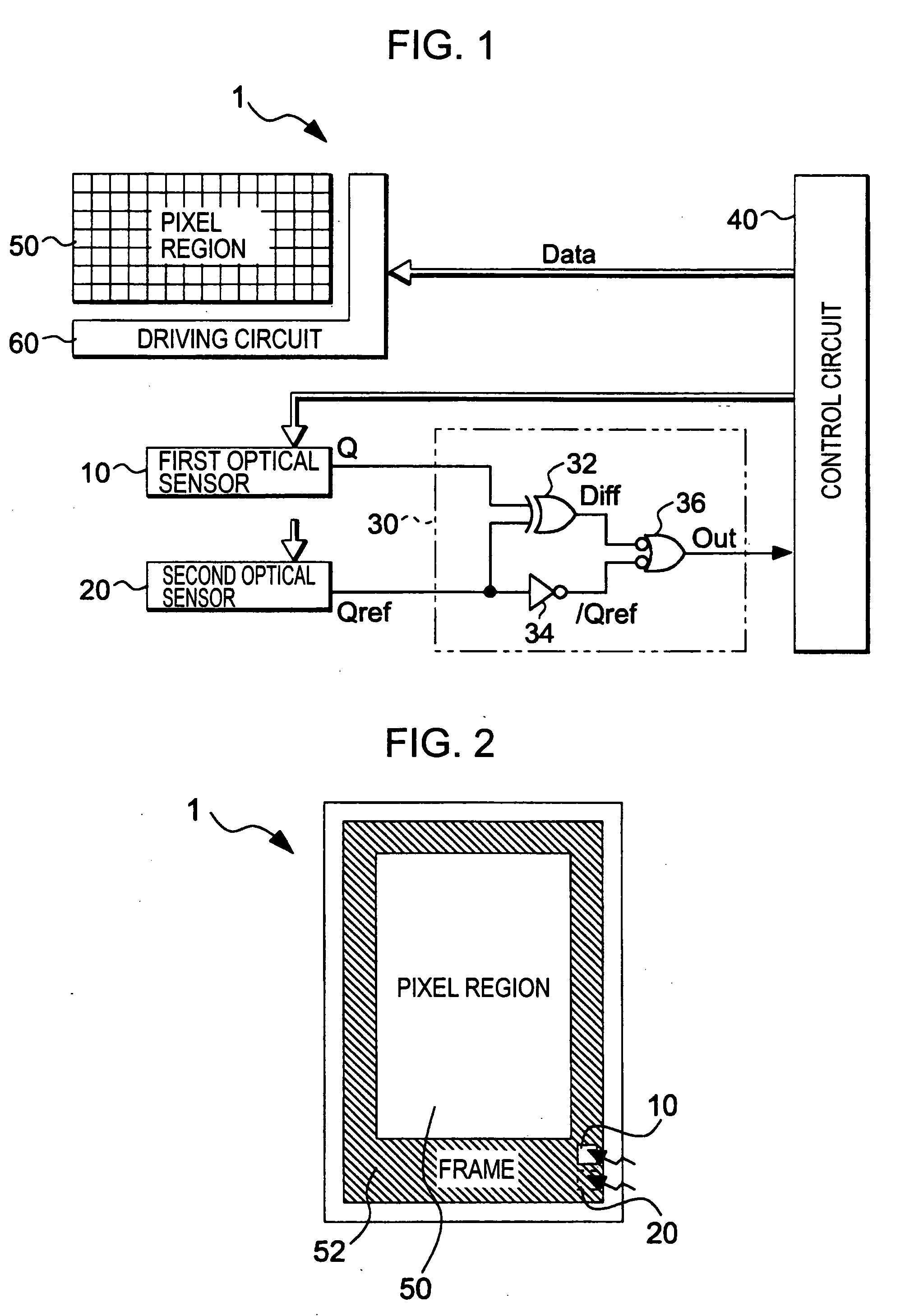
[0022]FIG. 1 is a block diagram showing the overall configuration of a liquid crystal display panel which has an optical sensor circuit according to an embodiment of the invention.

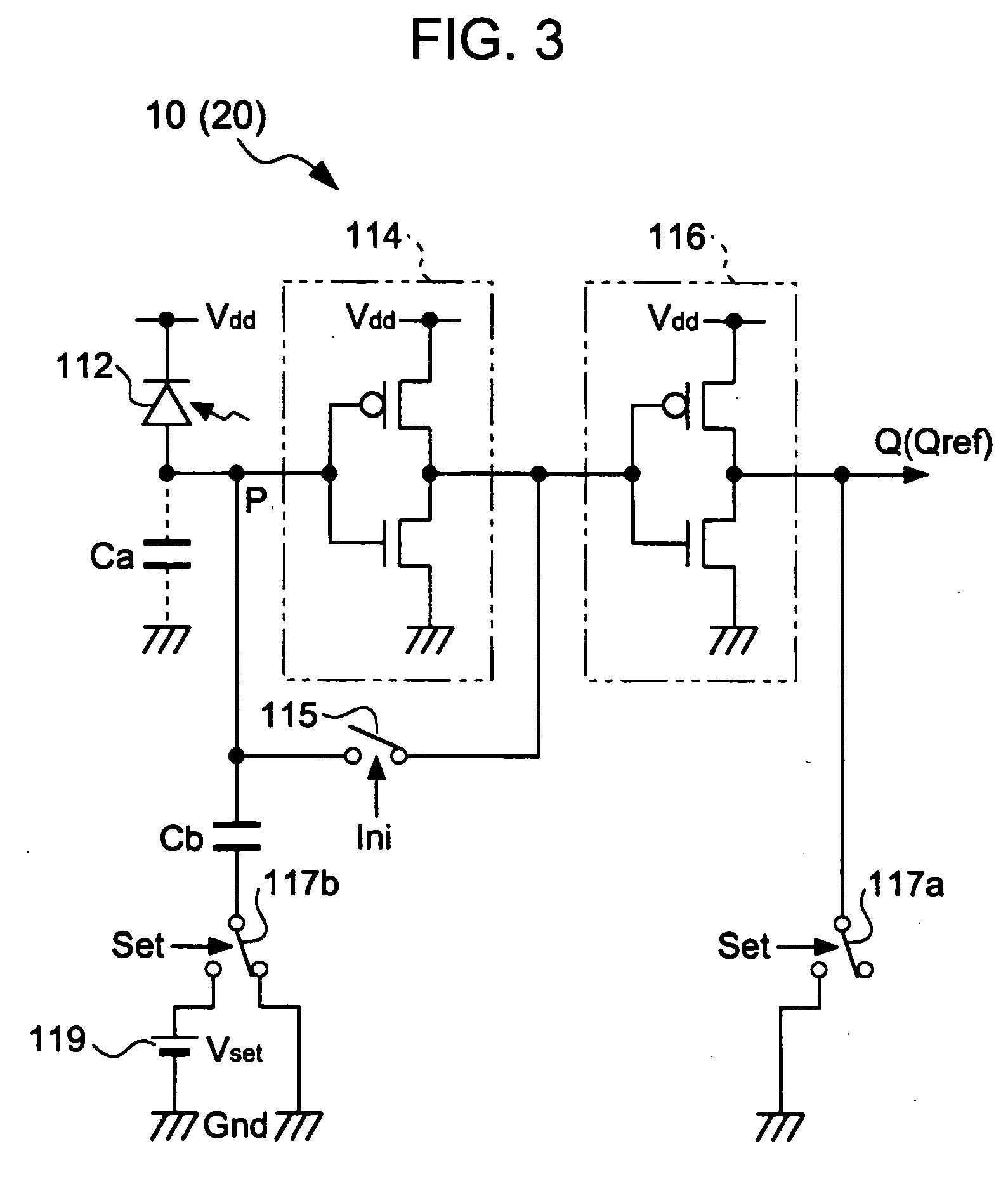
[0023] In FIG. 1, a first optical sensor 10 and a second optical sensor 20 output signals Q and Qref according to the amounts of received light, respectively. In the embodiment, the larger the amounts of received light received by the first optical sensor 10 and the second optical sensor 20, the smaller the pulse widths of Q and Qref are. The details will be described later. The first optical sensor 10 and the second optical sensor 20 are formed to be adjacent to each other on a region of the liquid crystal display panel 1 which corresponds to a frame 52 serving as a light-shielding layer which partitions an outer circumferential edge of a pixel region 50, as shown in FIG. 2. The first optical se...


PUM


Abstract

An optical sensor circuit has a first optical sensor that outputs a signal according to the amount of received light on an opened light-receiving surface, a second optical sensor that is provided near the first optical sensor and outputs a signal according to the amount of received light on a shielded light-receiving surface, and a difference calculating circuit that calculates a difference between the output signal of the first optical sensor and the output signal of the second optical sensor and outputs the difference.

Description

BACKGROUND OF THE INVENTION [0001] 1. Technical Field [0002] The present invention relates to a technique which reads an output of a light-receiving element such as a photodiode. [0003] 2. Related Art [0004] In recent years, a display panel in which liquid crystal elements or organic EL elements are arranged in a matrix shape has been widely been used for an electronic apparatus such as a cellular phone, a personal digital assistant, or the like. The display panel is used under various circumstances, for example, under bright conditions where there is sufficient sunlight, that is, daytime, or under dark conditions where external light is insufficient, that is, night. For this reason, when brightness or image quality of a display element is constant irregardless of external light, there is an inconsistency in that, while the display panel can be easily viewed under some conditions, it can hardly be viewed under other conditions. Accordingly, in such a display panel, it is preferable ...

Claims


Application Information

Patent Timeline
IPC IPC(8): H01L31/10G01J1/02G01J1/16G01J1/42G01J1/44G01J1/46H01J40/14H01L27/146H01L31/14
CPCG01J1/02G01J1/0271G01J1/1626H01L31/145G01J1/46G01J2001/444G01J1/4228H01L31/10
Inventor OZAWA, TOKURO
Owner 138 EAST LCD ADVANCEMENTS LTD
Learn More