Method for fabricating semiconductor device capable of scribing chips with high yield

a semiconductor device and high yield technology, applied in semiconductor devices, semiconductor/solid-state device details, electrical equipment, etc., can solve problems such as electrical shorts, partial exposure of wirings and electrodes, corrosion, etc., and achieve high manufacturing yield

Active Publication Date: 2005-12-08
FUJITSU LTD
View PDF7 Cites 135 Cited by
  • Summary
  • Abstract
  • Description
  • Claims
  • Application Information

AI Technical Summary

Benefits of technology

[0017] An object of this invention is to provide a method for fabricating a semiconductor device capable of dicing a scribe area with a high manufacture yield.

Problems solved by technology

Dicing a semiconductor water with a dicing saw poses sometimes the problem that the uppermost insulating layer of a semiconductor chip is wound around the dicing saw and cracked or peeled off, resulting in partial exposure of wirings and electrodes, electric short, corrosion and the like.

Method used


Image

  • Method for fabricating semiconductor device capable of scribing chips with high yield
  • Method for fabricating semiconductor device capable of scribing chips with high yield
  • Method for fabricating semiconductor device capable of scribing chips with high yield

Examples


Embodiment Construction

[0050] Prior to describing embodiments of the present invention, the study results made by the present inventor will be described.

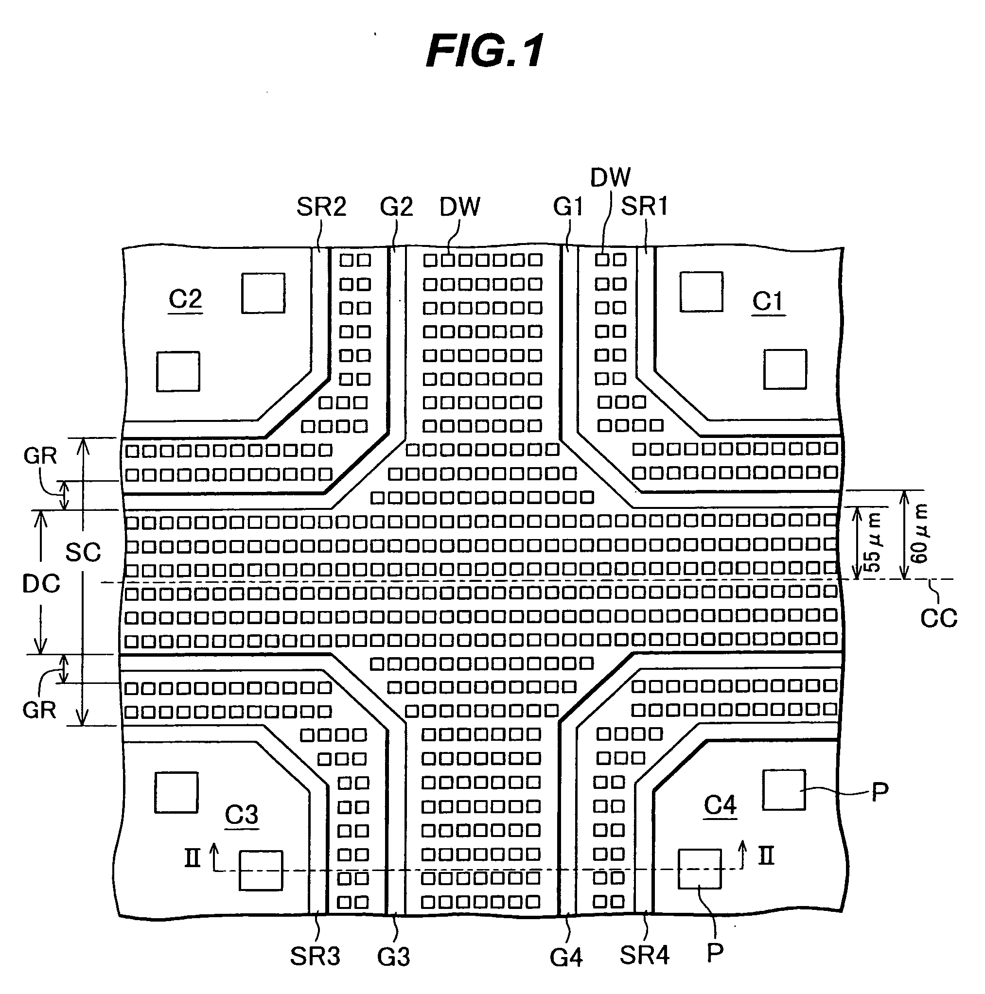
[0051] If dummy wirings are disposed also in the scribe area as in the structure shown in FIG. 22B, the flatness of the whole wafer surface can be easily realized. Similar to the pad—peripheral circuit area, dummy wirings are disposed in the scribe area and covered with the cover layer including the passivation layer 125.

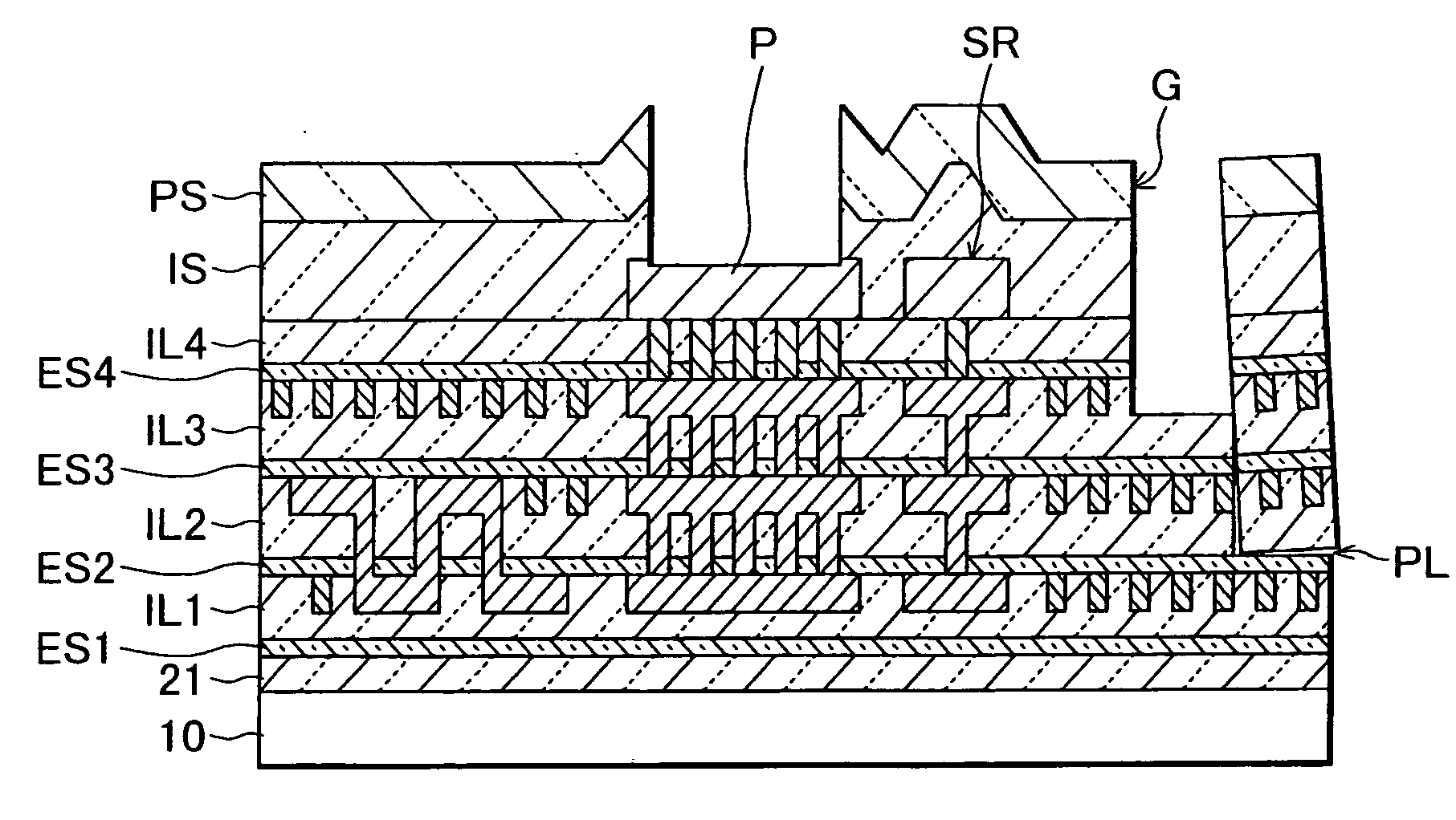
[0052]FIG. 23 is a schematic cross sectional view showing the structure of a semiconductor device actually used for the studies by the present inventor. Semiconductor elements are formed on a semiconductor substrate 10 and covered with an insulating layer 21. A multilayer wiring is formed on the insulating layer 21. A lamination of the multilayer wiring insulation layer includes an interlayer insulating film IL1, an etch stopper and copper diffusion preventive layer ES2, an interlayer insulating film IL2, an etch stopper and copper diff...


PUM


Abstract

A method for fabricating a semiconductor device in which a scribe area can be diced with high yield. The method for fabricating a semiconductor device comprises (a) a step for providing a semiconductor wafer having a plurality of chip areas in which semiconductor elements are formed, and a scribe area for separating the plurality of chip areas and including dicing areas with groove forming areas being defined to surround each chip area on the outer side of the dicing area in the scribe area, (b) a step for arranging a multilayer interconnection structure where interlayer insulation films and interconnection layers are formed alternately above the semiconductor wafer along with dummy lines, (c) a step for forming a cover layer covering the multilayer interconnection structure and including a passivation layer, and (d) a step for forming a groove surrounding each of the plurality of chip areas and penetrating at least the passivation layer from above in the groove forming area.

Description

CROSS REFERENCE TO RELATED APPLICATION [0001] This application is a continuation application of PCT / JP2004 / 000583 filed on Jan. 23, 2004, which claims priority of PCT / JP03 / 05514 filed on Apr. 30, 2003, the entire contents of which are incorporated herein by reference.BACKGROUND OF THE INVENTION [0002] A) Field of the Invention [0003] The present invention relates to a method for fabricating a semiconductor device, a semiconductor wafer and a semiconductor device, and more particularly to a method for fabricating a semiconductor device having a multilayer wiring structure, a semiconductor wafer and a semiconductor device. [0004] B) Description of the Related Art [0005] In fabricating a semiconductor integrated circuit device, a number of chip areas divided by a scribe area are defined in a semiconductor wafer. Semiconductor elements are formed in each chip area, and an interconnection or wiring layer and an interlayer insulating layer are alternately stacked in each chip area. After ...

Claims


Application Information

Patent Timeline
Patent Type & Authority Applications(United States)
IPC IPC(8): H01L21/301H01L21/3205H01L21/768H01L21/78H01L23/485H01L23/522H01L23/544H01L23/58
CPCH01L21/76801H01L21/76808H01L2924/0002H01L2924/00014H01L2924/13091H01L2224/05554H01L2224/02166H01L2924/01021H01L2924/01019H01L21/76819H01L21/76838H01L21/78H01L23/522H01L23/585H01L24/03H01L24/05H01L2224/0401H01L2224/04042H01L2224/05093H01L2224/05567H01L2224/05624H01L2924/01002H01L2924/01005H01L2924/01006H01L2924/01013H01L2924/01014H01L2924/01015H01L2924/01018H01L2924/01022H01L2924/01029H01L2924/01033H01L2924/01038H01L2924/0105H01L2924/01059H01L2924/01073H01L2924/01074H01L2924/01078H01L2924/01082H01L2924/05042H01L2924/14H01L2924/19043H01L2924/30105H01L2924/3025H01L2924/00H01L2224/05552H01L21/76811H01L21/30H01L21/3205
Inventor OTSUKA, SATOSHI
Owner FUJITSU LTD
Why Eureka
Try Eureka