

Display device and method of manufacturing the same
a technology of display device and display device, which is applied in the direction of static indicating device, electroluminescent light source, instruments, etc., can solve the problem of easily delayed current through interconnection
- Summary
- Abstract
- Description
- Claims
- Application Information
AI Technical Summary
Benefits of technology
Problems solved by technology
Method used
Image

Examples
first embodiment
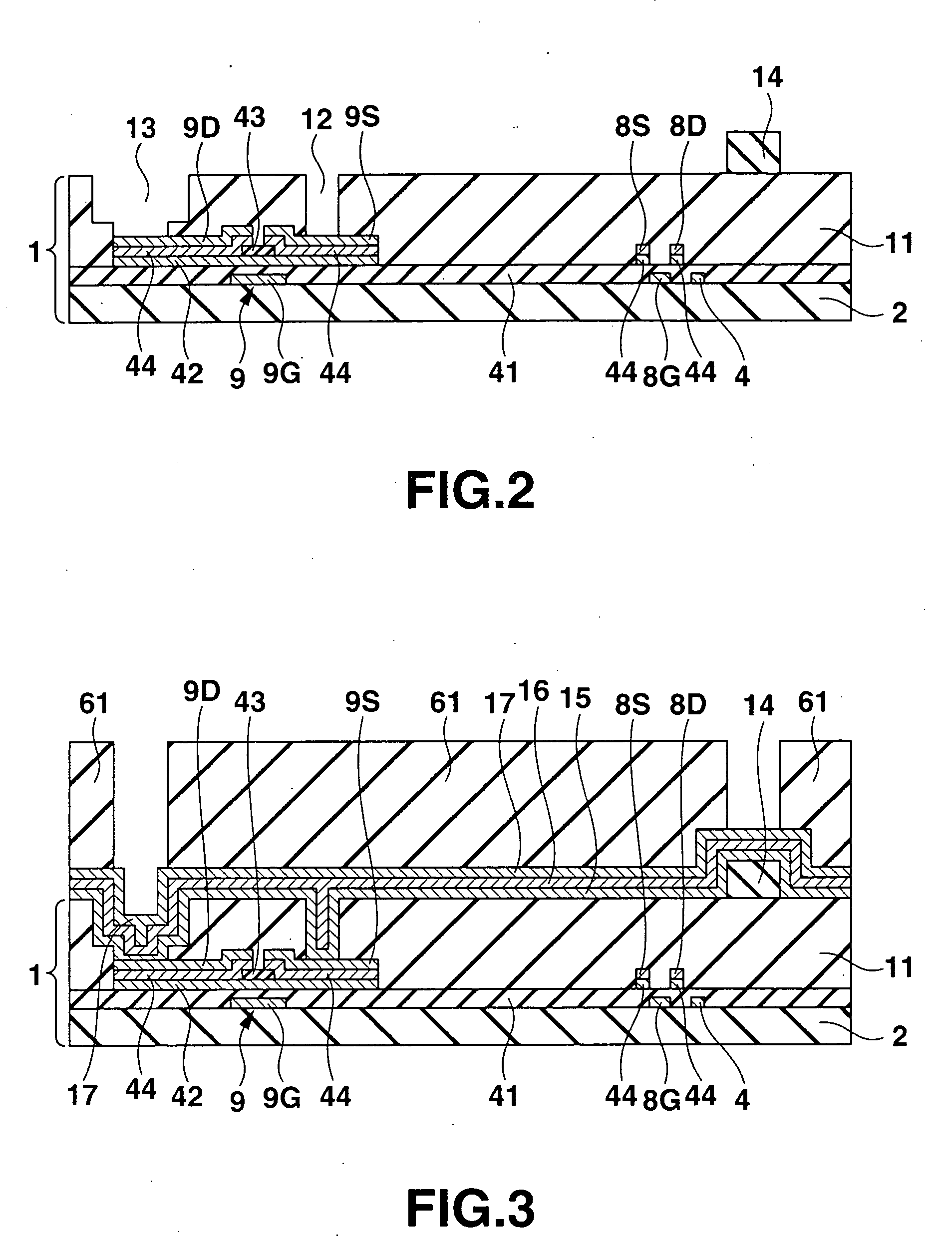
[0099] A method of manufacturing a display device having, as pixels, organic electroluminescent elements serving as light-emitting elements will be described with reference to FIGS. 2 to 7. FIGS. 2 to 7 are sectional views of steps in the manufacturing method. The steps are executed in the order of FIGS. 2 to 7.
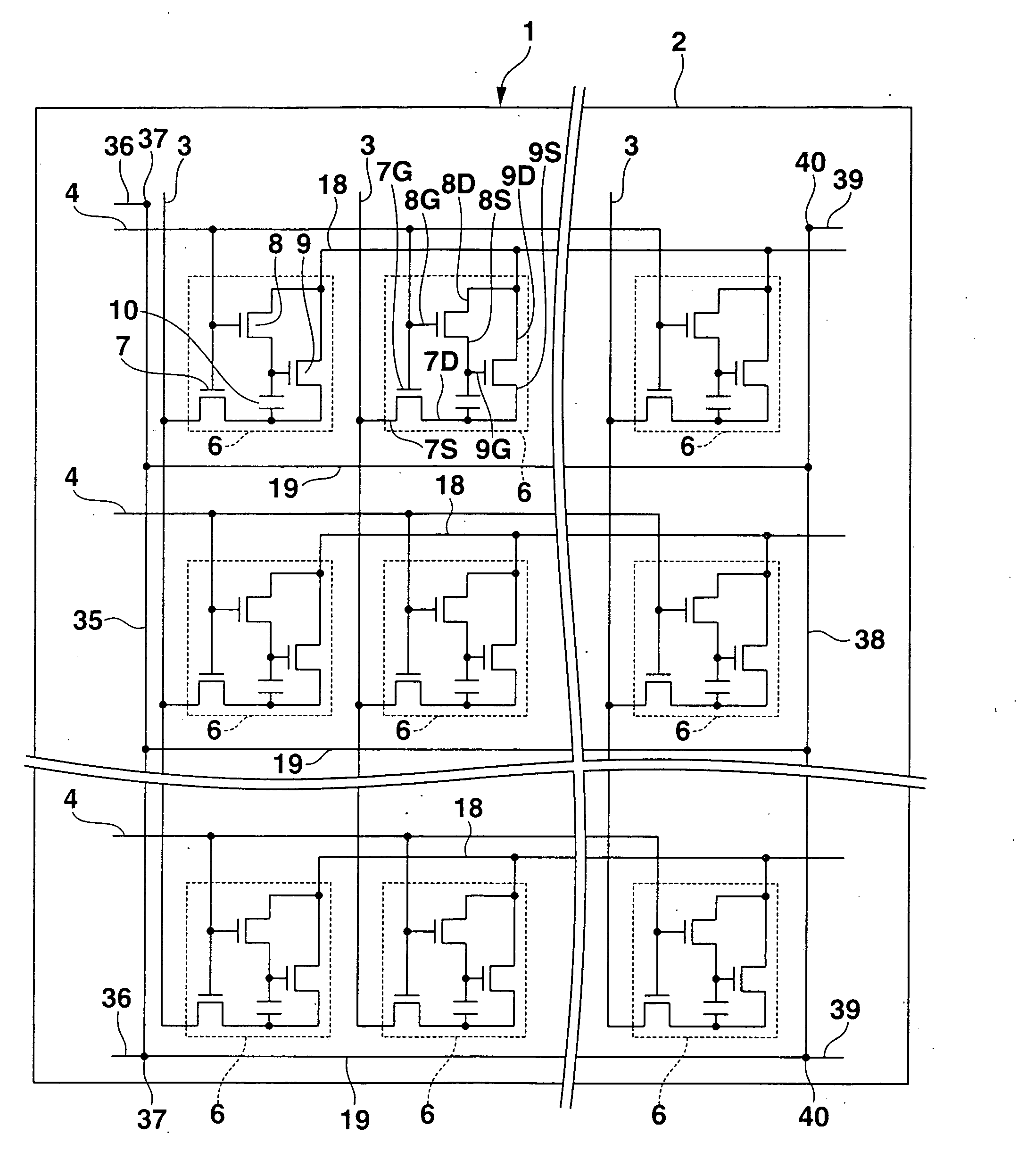
[0100] A transistor array substrate 1 having pixel circuits, as shown in FIGS. 1 and 2 is manufactured. The transistor array substrate 1 is a current luminance gray level control panel. A pixel circuit 6 does not execute voltage luminance gray level control by a signal voltage, unlike the prior art. Instead, a luminance gray level current (storage current) having a current value corresponding to luminance gray level data is supplied into the pixel circuit 6 to generate a driving current having a current value corresponding to the current value of the luminance gray level current. The driving current is supplied to an organic EL element 26 (to be described later) to control t...
second embodiment
[0143] A method of manufacturing a display device according to the second embodiment will be described with reference to FIGS. 11 to 16. FIGS. 11 to 16 are sectional views of steps in the manufacturing method. The steps are executed in the order of FIGS. 11 to 16. The same reference numerals as in the display device of the first embodiment denote the same parts in FIGS. 11 to 16, and some of the same steps as in the first embodiment are not illustrated.
[0144] As shown in FIG. 11, a transistor array substrate 1 is manufactured. A reflecting metal film 15d is patterned on a planarizing film 11 for each pixel by executing a reflecting metal film forming process such as vapor deposition, a mask process such as photolithography, and a shaping process such as etching in this order.
[0145] A transparent insulating film 131 is formed on the entire surface by vapor deposition to cover the reflecting metal film 15d. The reflecting metal film 15d is electrically insulated by the transparent i...
third embodiment
[0157] A method of manufacturing an electroluminescent display panel according to the third embodiment will be described with reference to FIGS. 17 to 22. FIGS. 17 to 22 are sectional views of steps in the manufacturing method. The steps are executed in the order of FIGS. 17 to 22. The same reference numerals as in the electroluminescent display panel of the second embodiment denote the same parts in FIGS. 17 to 22, and some of the same steps as in the first embodiment are not illustrated.
[0158] As shown in FIG. 17, a transistor array substrate 1 is manufactured. A reflecting metal film 15d is patterned on a planarizing film 11 for each pixel by executing a reflecting metal film forming process such as vapor deposition including sputtering, a mask process such as photolithography, and a shaping process such as etching in this order.
[0159] A transparent insulating film 131 is formed on the entire surface by vapor deposition to cover the reflecting metal film 15d. The reflecting met...
PUM
 Abstract
Description
Claims
Application Information