

Nonvolatile semiconductor memory
a semiconductor memory and non-volatile technology, applied in semiconductor devices, digital storage, instruments, etc., can solve problems such as the potential for the selected word line in a selected block to rise in error, and achieve the effect of reducing the resistance in the contact area
- Summary
- Abstract
- Description
- Claims
- Application Information
AI Technical Summary
Benefits of technology
Problems solved by technology
Method used
Image

Examples
first embodiment
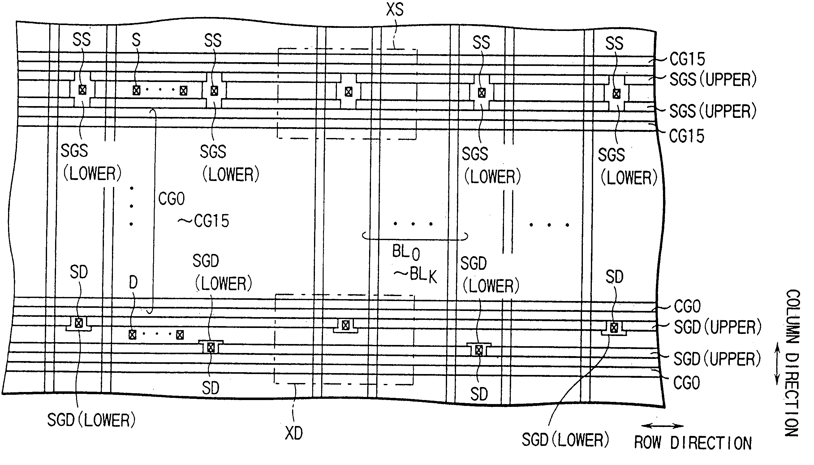
[0454]FIG. 104 shows pattern of a NAND cell EEPROM of the present invention. FIG. 105 is a view showing the inside of the area A1 of FIG. 104 in detail. FIG. 106 is a view showing the inside of the area A2 of FIG. 104.
[0455] A memory cell array is constructed of a plurality of blocks BLOCK i−1, BLOCK i, BLOCK i+1, . . . . A plurality of word lines (control gate lines=control gate electrodes) CG1 to CG8 and select gate lines SG1 and SG2 extending in the row direction are located in each block. A plurality of bit lines BL extending in the column direction are shared in common with each block.
[0456] Shunt areas QQ are located at constant intervals in the row direction. In a shunt area, select gate lines. SG1 and SG2 are connected to select gate bypass lines 21i and 21i−1, which are formed above the select gate lines SG1 and SG2, and whose resistances are lower than each of the select gate lines SG1 and SG2. In the example, the case where the select gate bypass lines 21i and 21i−1 are ...
second embodiment
[0505]FIGS. 114 and 115 show pattern of a NAND cell EEPROM of the present invention. FIG. 114 is a view in detail showing the area A1 of FIG. 104, and FIG. 115 is a view in detail showing the area A2 of FIG. 104.
[0506] An EEPROM of the example will be compared with the EEPROM of the first embodiment described above. The EEPROM of the second embodiment is different from the first embodiment in that a select gate bypass line which is connected to a select gate line SG1 in a selected BLOCK block is existent in the selected block.
[0507] That is, a select gate bypass line 21i−1 which is connected to a select gate line SG1 in a block BLOCK I−1 is located in the block BLOCK i−1 and a select gate bypass line 21i which is connected to a select gate line SG1 in a block BLOCK i is located in the block BLOCK i.
[0508] A feature of the EEPROM of the second embodiment resides in the following points.
[0509] The select gate bypass lines 21i−1 and 21i are located in the drain side (bit contact sec...
third embodiment
[0514]FIG. 117 shows pattern of a NAND cell EEPROM of the present invention. FIG. 117 is a view in detail showing the area A1 of FIG. 104. In the example, a figure corresponding to the area A2 of FIG. 104 is omitted.
[0515] The EEPROM of the example will be compared with the EEPROM of the second embodiment. It is same as the second embodiment that a select gate bypass line which is connected to a select gate line SG1 in a selected BLOCK block is existent in the selected block, whereas it is different from the second embodiment that the source side edges of select gate bypass lines 21i−1 and 21i are both located between the drain side edge of a word line (control gate electrode) CG1 closest to the drain (bit line contact section) and the source side edge of a select gate line SG1.
[0516] In other words, select gate bypass lines 21i−1 and 21i which are connected to a select gate line SG1 are located in the drain side (bit line contact section) further away from the drain side edge of a...
PUM
 Abstract
Description
Claims
Application Information