Method and structure for reducing contact resistance between silicide contact and overlying metallization

a technology of contact resistance and silicide, applied in the field of silicide structure, can solve the problems of increasing the number of contacts, affecting the device previously fabricated, and the difficulty of filling via holes, so as to reduce the contact resistance in the contact opening

Inactive Publication Date: 2007-11-29
GLOBALFOUNDRIES INC
View PDF7 Cites 36 Cited by
  • Summary
  • Abstract
  • Description
  • Claims
  • Application Information

AI Technical Summary

Benefits of technology

[0011]The present invention provides a semiconductor structure in which the contact resistance in the contact opening is reduced. This is achieved in the present invention by replacing conventional contact metallurgy, such as tungsten, or a metal silicide, such as Ni silicide or Cu silicide, with a metal germanide-containing contact material. The term “metal germanide-containing” is used in the present application to denote a pure metal germanide (i.e., MGe alloy) or a metal germanide that includes Si (i.e., MSiGe alloy).

Problems solved by technology

Although tungsten possesses a low bulk resistivity (5.5 μΩ-cm), the bulk via resistance is also affected by the presence of voids or seams within the via, a problem that becomes more prevalent as via holes become more difficult to fill using conventional deposition techniques, such as chemical vapor deposition (CVD).
This problem represents a significant impact on the performance and development of semiconductor technology.
One problem with this prior art approach is that the Ni silicide is formed at a relatively high temperature which may adversely affect the device previously fabricated.

Method used


Image

  • Method and structure for reducing contact resistance between silicide contact and overlying metallization
  • Method and structure for reducing contact resistance between silicide contact and overlying metallization
  • Method and structure for reducing contact resistance between silicide contact and overlying metallization

Examples


Embodiment Construction

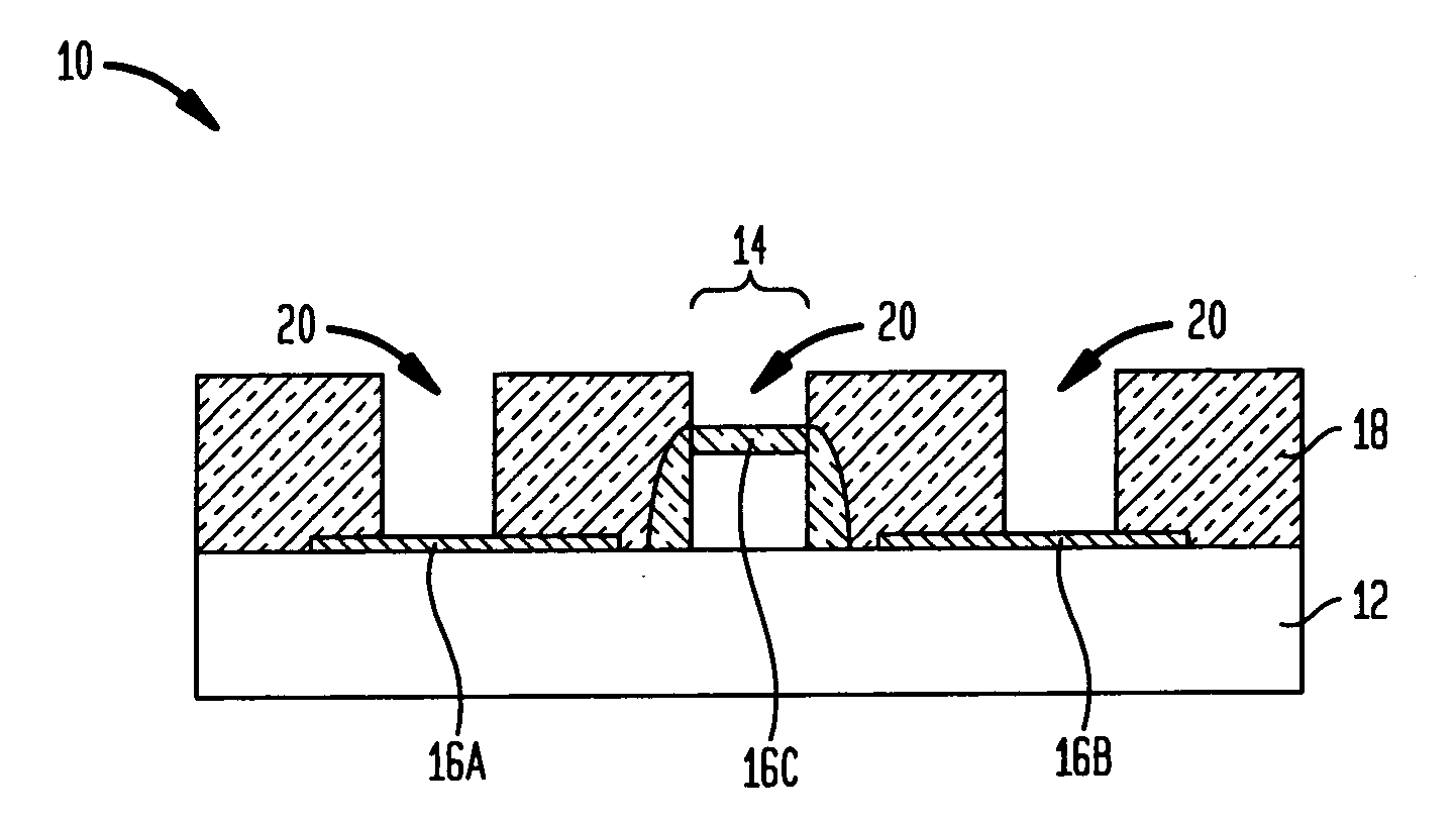
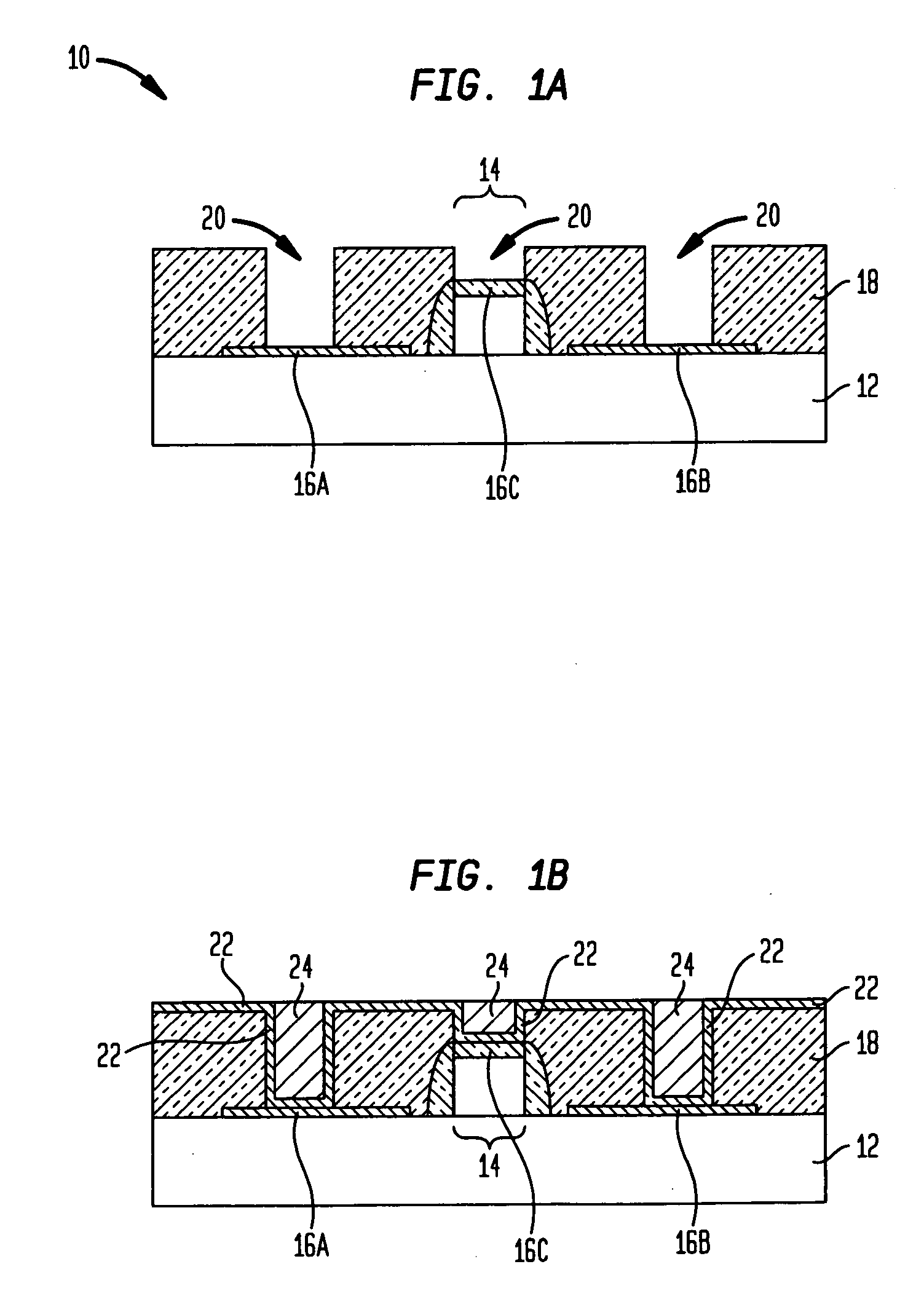
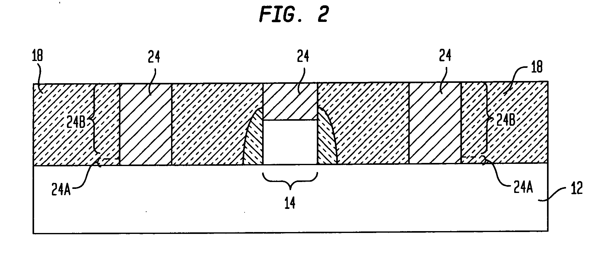
[0038]The present invention, which provides a semiconductor structure having reduced contact resistance in a contact opening as well as a method of forming the same, will now be described in greater detail by referring to the following discussion and drawings that accompany the present application. The drawings of the present application, which are referred to herein below in greater detail, are provided for illustrative purposes and, as such, they are not drawn to scale.

[0039]In the following description, numerous specific details are set forth, such as particular structures, components, materials, dimensions, processing steps and techniques, in order to provide a thorough understanding of the present invention. However, it will be appreciated by one of ordinary skill in the art that the invention may be practiced without these specific details. In other instances, well-known structures or processing steps have not been described in detail in order to avoid obscuring the invention....


PUM

PropertyMeasurementUnit
temperatureaaaaaaaaaa
dielectric constantaaaaaaaaaa

Abstract

A semiconductor structure in which the contact resistance in the contact opening is reduced as well as a method of forming the same are provided. This is achieved in the present invention by replacing conventional contact metallurgy, such as tungsten, or a metal silicide, such as Ni silicide or Cu silicide, with a metal germanide-containing contact material. The term “metal germanide-containing” is used in the present application to denote a pure metal germanide (i.e., MGe alloy) or a metal germanide that includes Si (i.e., MSiGe alloy).

Description

FIELD OF THE INVENTION[0001]The present invention relates to a semiconductor structure and a method of fabricating the same. More particularly, the present invention relates to a semiconductor structure in which the contact resistance in the contact opening, typically between the silicide contact and the overlying metallization, is reduced. The present invention also relates to a method of fabricating such a semiconductor structure.BACKGROUND OF THE INVENTION[0002]In order to meet the ever increasing demand for increased device density and performance, a semiconductor technology consisting of a low-k dielectric material (dielectric constant less than silicon dioxide) and an interconnection wiring of copper metallurgy, defined by a double damascene method, is the present day choice for the back end of line (BEOL). Because, dry air has the theoretically lowest dielectric constant of one (1), most low-k materials such as aerogels, hydrogen silsesquioxane (HSQ), fluorinated organic poly...

Claims


Application Information

Patent Timeline
Patent Type & Authority Applications(United States)
IPC IPC(8): H01L21/44
CPCH01L21/28518H01L21/76877H01L21/76883H01L23/485H01L23/53209H01L2924/0002H01L2924/12044H01L2924/00
Inventor LAVOIE, CHRISTIANMURRAY, CONAL E.RODBELL, KENNETH P.
Owner GLOBALFOUNDRIES INC
Why Eureka
Try Eureka