Method of depositing low resistivity barrier layers for copper interconnects

a copper interconnection and resistivity barrier technology, applied in vacuum evaporation coatings, sputtering coatings, coatings, etc., can solve the problem of difficult to obtain precisely the desired nitrogen content in the seed layer, and achieve the effect of high energy species

Inactive Publication Date: 2005-12-08
APPLIED MATERIALS INC
View PDF99 Cites 50 Cited by
  • Summary
  • Abstract
  • Description
  • Claims
  • Application Information

AI Technical Summary

Benefits of technology

[0020] In another embodiment of the method of forming a TaN seed layer, a tantalum film is deposited on a semiconductor substrate surface, and then the surface of the Ta film is bombarded with high energy species while in contact with a nitrogen-containing plasma. The thickness of the Ta layer may range from about 5 Å to about 500 Å. Small amounts of reactive tantalum species, which are liberated from the tantalum film surface due to the high energy species bombardment, react with or trap nitrogen from a plasma present over the tantalum film surface, and redeposit on the tantalum film surface to provide a TaN seed layer, having a nominal nitrogen content between about 5 atomic % and about 33 atomic %, and typically less than about 15 atomic %. After formation of at least two monolayers of TaN seed layer material, nitrogen is removed from the plasma present over the TaN seed layer surface. Tantalum subsequently deposited over the TaN seed layer surface is alpha-tantalum. The TaN seed layer typically ranges from about 2 monolayers to about 10 monolayers, which provides a TaN seed layer thickness ranging from about 2 Å to about 100 Å, more typically about 20 Å to about 100 Å. The plasma density and the voltage on the substrate surface are controlled so that the amount of energy transferred to the Ta film surface is sufficient to cause Ta species to rise into the space above the Ta film surface, where the nitrogen species from the plasma contact and react with the tantalum species. This forms TaN atoms, and the TaN atoms thus formed settle down on the Ta surface, forming a TaN seed layer. Controlling the plasma density and the voltage on the substrate enables applicants to control the amount of energy that is transferred to the substrate and ensures that the transferred energy is sufficient to provide Ta species for reaction with nitrogen in the plasma, without sputtering Ta from the Ta film surface onto adjacent non-tantalum containing surfaces. In general, resputtering does not occur or is minimal; typically, less than 10% of the original Ta film thickness is altered.

Problems solved by technology

Since the seed layer is typically about 2-10 monolayers thick, it is difficult to obtain precisely the desired nitrogen content in the seed layer.

Method used


Image

  • Method of depositing low resistivity barrier layers for copper interconnects
  • Method of depositing low resistivity barrier layers for copper interconnects
  • Method of depositing low resistivity barrier layers for copper interconnects

Examples


Embodiment Construction

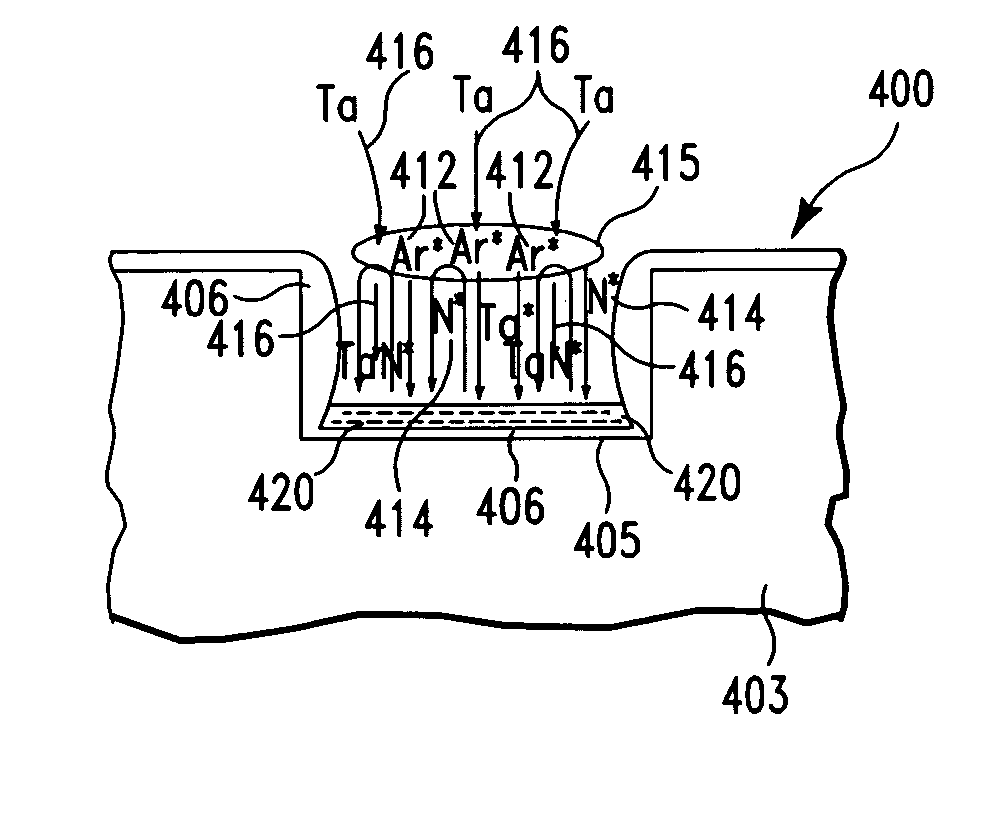
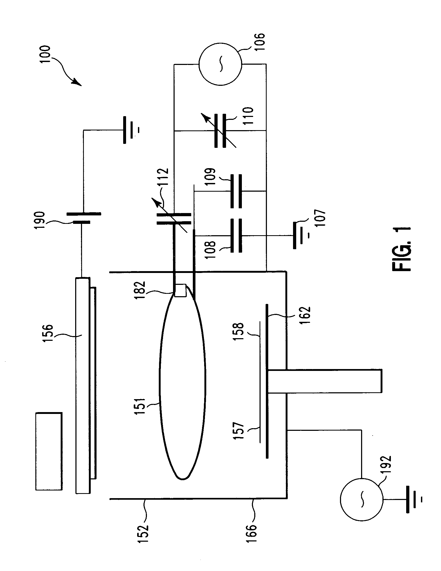
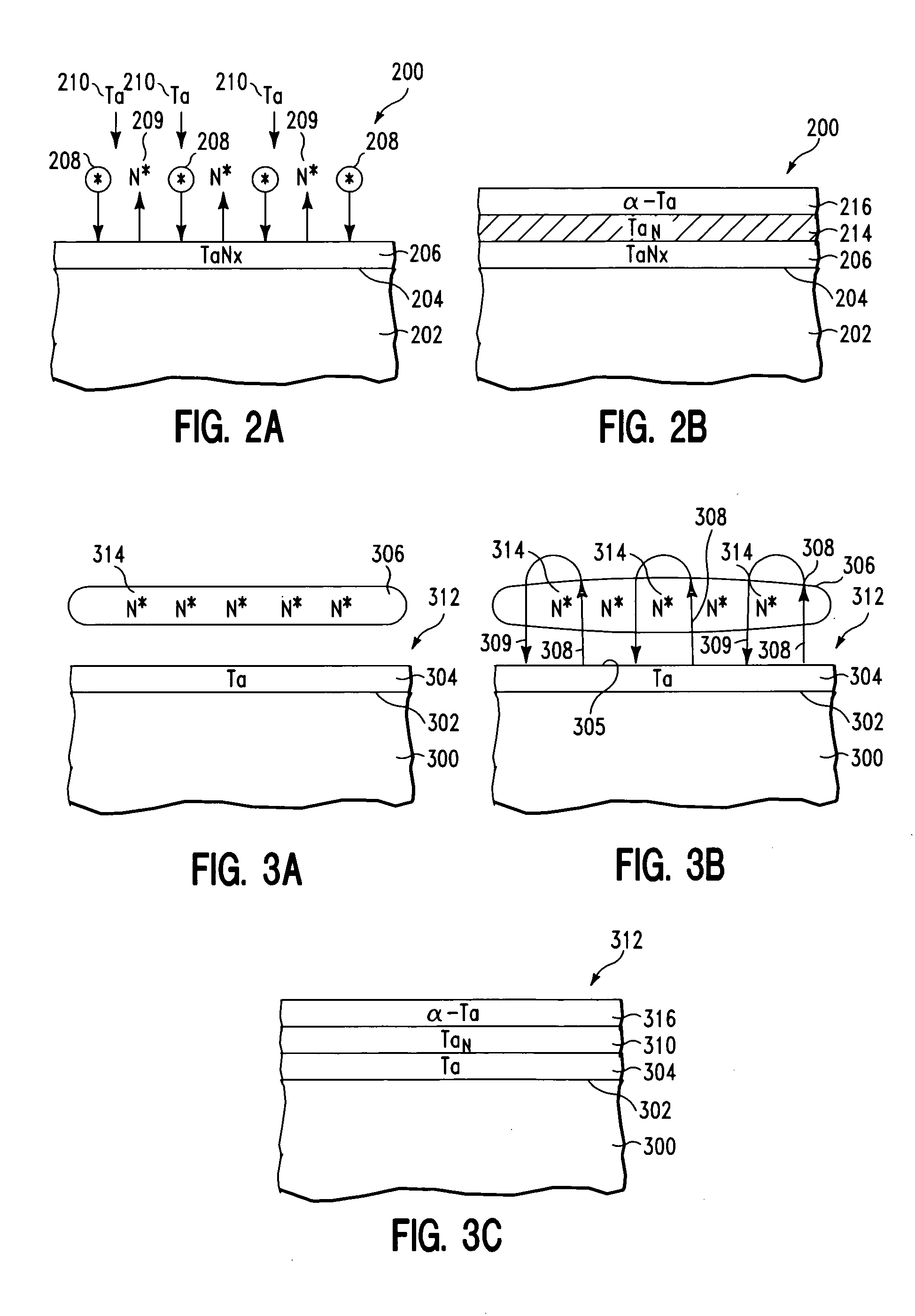
[0046] This application is a continuation-in-part of U.S. patent application Ser. No. 10 / 246,316, filed Sep. 17, 2002, which is allowed but not yet issued; which is a continuation-in-part of U.S. patent application Ser. No. 10 / 146,416, filed May 14, 2002, which is abandoned; which is a continuation of U.S. patent application Ser. No. 09 / 770,934, filed Jan. 25, 2001, which issued as U.S. Pat. No. 6,458,255, on Oct. 1, 2002; which is a continuation of U.S. patent application Ser. No. 09 / 160,638, filed Sep. 24, 1998, which is abandoned. This application is also a continuation-in-part of U.S. patent application Ser. No. 08 / 995,108, filed Dec. 19, 1997, which is allowed but not yet issued. This application is also a continuation-in-part of U.S. patent application Ser. No. 10 / 796,602, filed Mar. 8, 2004, which is allowed but not yet issued; which is a continuation of U.S. patent application Ser. No. 09 / 886,439, filed Jun. 20, 2001, which issued as U.S. Pat. No. 6,758,947, on Jul. 6, 2004;...


PUM

PropertyMeasurementUnit
poweraaaaaaaaaa
poweraaaaaaaaaa
sizesaaaaaaaaaa

Abstract

We have discovered a method of providing a thin approximately from about 2 Å to about 100 Å thick TaN seed layer, which can be used to induce the formation of alpha tantalum when tantalum is deposited over the TaN seed layer. Further, the TaN seed layer exhibits low resistivity, in the range of 30 μΩ cm and can be used as a low resistivity barrier layer in the absence of an alpha tantalum layer. In one embodiment of the method, a TaN film is altered on its surface form the TaN seed layer. In another embodiment of the method, a Ta film is altered on its surface to form the TaN seed layer.

Description

[0001] This application is a continuation-in-part of U.S. patent application Ser. No. 10 / 246,316, filed Sep. 17, 2002, which is allowed but not yet issued; which is a continuation-in-part of U.S. patent application Ser. No. 10 / 146,416, filed May 14, 2002, which is abandoned; which is a continuation of U.S. patent application Ser. No. 09 / 770,934, filed Jan. 25, 2001, which issued as U.S. Pat. No. 6,458,255, on Oct. 1, 2002; which is a continuation of U.S. patent application Ser. No. 09 / 160,638, filed Sep. 24, 1998, which is abandoned. Application Ser. No. 10 / 246,316 is hereby incorporated by reference in its entirety. This application is also a continuation-in-part of U.S. patent application Ser. No. 08 / 995,108, filed Dec. 19, 1997, which is allowed but not yet issued. Application Ser. No. 08 / 995,108 is hereby incorporated by reference in its entirety. This application is also a continuation-in-part of U.S. patent application Ser. No. 10 / 796,602, filed Mar. 8, 2004, which is allowed ...

Claims


Application Information

Patent Timeline
Patent Type & Authority Applications(United States)
IPC IPC(8): C23C14/06C23C14/16C23C14/32H01L21/285H01L21/44H01L21/4763H01L21/768
CPCC23C14/0641C23C14/165C23C14/541C23C14/5806H01L21/76876H01L21/318H01L21/76846H01L21/76856H01L21/76862H01L21/2855H01L21/02266H01L21/02183
Inventor DING, PEIJUNXU, ZHENGZHANG, HONGTANG, XIANMINGOPALRAJA, PRABURAMRENGARAJAN, SURAJFORSTER, JOHN C.FU, JIANMINGCHIANG, TONYYAO, GONGDACHEN, FUSEN E.CHIN, BARRY L.KOHARA, GENE Y.
Owner APPLIED MATERIALS INC
Why Eureka
Try Eureka