Method for evaluating semiconductor device

a semiconductor and device technology, applied in the direction of testing circuits, instruments, nuclear elements, etc., can solve the problems of difficult statistical determination, adversely affecting the integrated circuit, and difficult to identify the cause of failure, so as to achieve efficient measurement

Inactive Publication Date: 2005-12-08
SEMICON ENERGY LAB CO LTD
View PDF2 Cites 37 Cited by
  • Summary
  • Abstract
  • Description
  • Claims
  • Application Information

AI Technical Summary

Benefits of technology

[0017] By providing a plurality of circuits and a selection circuit over the same substrate, measurement can be carried out efficiently. In addition, by providing the plurality of circuits and the selection circuit over the same substrate, evaluation can be performed precisely.

Problems solved by technology

However, when failures are caused, e.g., the integrated circuit does not work, since the integrated circuit includes too many semiconductor elements, it is very difficult to identify a cause of failures.
However, it is difficult to statistically determine parameters by using one TEG Also, there are many parameters that adversely affect an integrated circuit.
Therefore, in order to find out parameters that can operate an integrated circuit stably in designing the integrated circuit, enormous numbers of TEGs must be manufactured by way of trial and evaluated, thereby involving a lot of time and effort to produce.
Moreover, it is very difficult to separate an influence of variation caused by the difference of lots for manufacturing TEGs from an influence due to change of intended parameters.

Method used


Image

  • Method for evaluating semiconductor device
  • Method for evaluating semiconductor device
  • Method for evaluating semiconductor device

Examples


embodiment mode 1

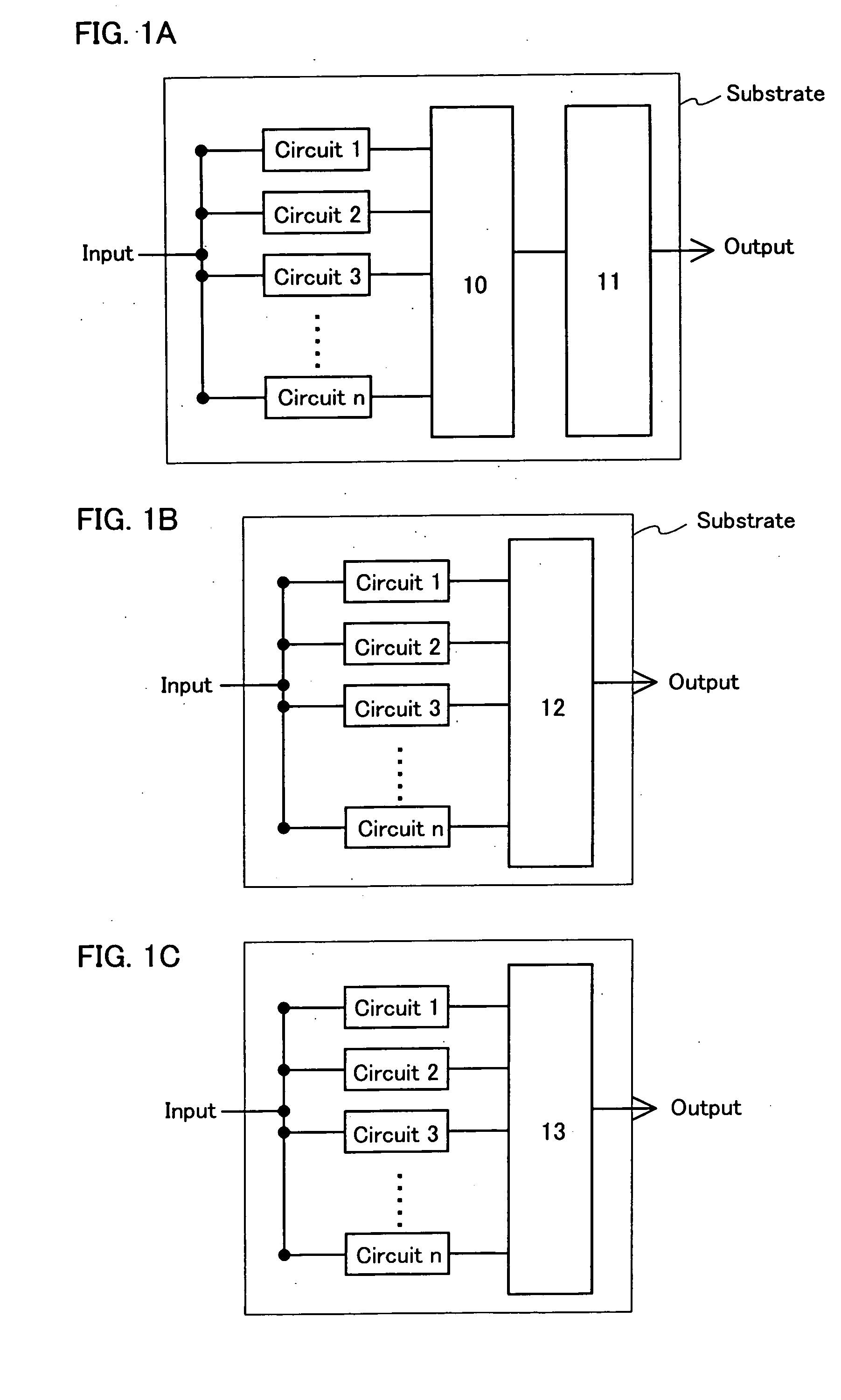
[0027]FIG. 1A shows a substrate for evaluation comprising a plurality of evaluation circuits, a selection circuit 10 and a determination circuit 11. Data output from n pieces of evaluation circuits is input in the same selection circuit 10. Data output from the selection circuit 10 is input in the determination circuit 11. The evaluation circuits 1 to n may comprise either the same circuit configuration or different configurations from one another. When the evaluation circuits comprise the same circuit configuration, circuit parameters such as resistance, capacitance and inductance may be differed in the respective circuits. When using evaluation circuits having the same circuit configuration, operations of the plurality of evaluation circuits can simultaneously be evaluated. On the other hand, when using evaluation circuits having different circuit parameters, a plurality of test parameters can simultaneously be evaluated.

[0028] The substrate for evaluation as shown in FIG. 1A has...

embodiment mode 2

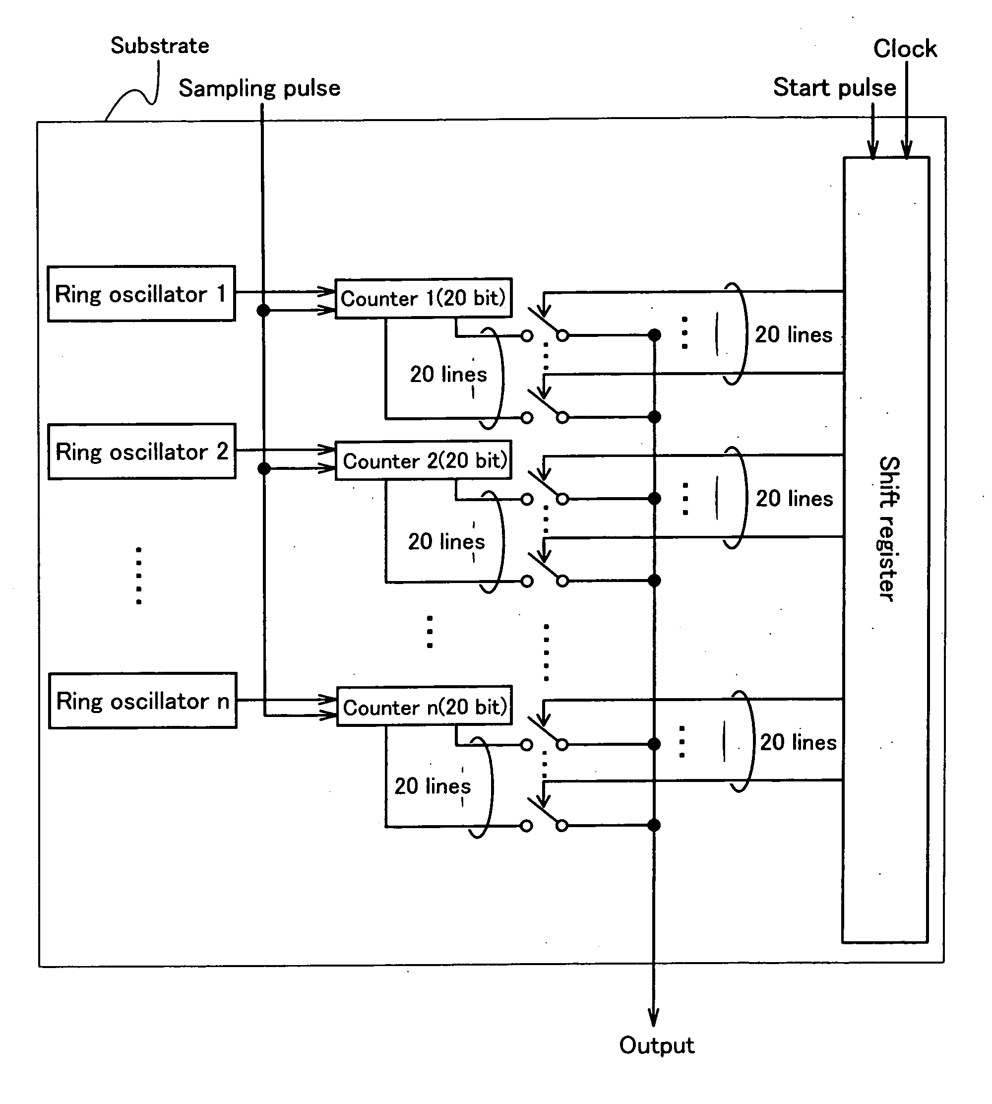
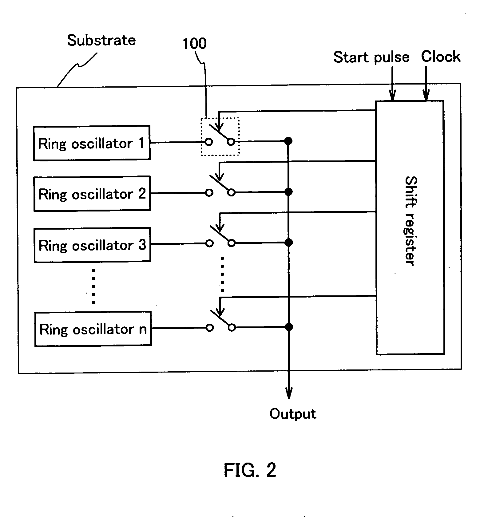
[0042] An influence of different output load (i.e., stress to be applied is differed due to difference of a delay situation of a waveform) will be examined in the present embodiment mode by forming a substrate for evaluation of the invention and by using n pieces of similar ring oscillators in which capacitance of the respective ring oscillators is changed stepwise. An analog output is employed. This embodiment mode will be described with reference to FIG. 2.

[0043] One purpose of this embodiment mode is that deteriorated properties of the various ring oscillators are evaluated. The deteriorated properties of the ring oscillators with different output load or the different number of stages (number of inverters) of each logic gate are evaluated respectively and compared with a deteriorated property of a more complicated logic circuit, and hence, the deteriorated property of the more complicated logic circuit can be evaluated easily.

[0044] A substrate for evaluation according to the ...

embodiment mode 3

[0055] The present embodiment mode shows a configuration in which n pieces of the same ring oscillators are provided as a plurality of circuits over a substrate for evaluation according to the invention so as to examine an influence due to variation in semiconductor elements included in the ring oscillators. An analog output is employed. This embodiment mode will be described with reference to FIG. 2.

[0056] The variation in reliability of the semiconductor elements such as thin film transistors that are included in the ring oscillators is assumed as one of reasons why a result of the deterioration caused in one ring oscillator is differed of a result of the deterioration caused in a CPU. In order to examine the influence of the variation in reliability of the semiconductor elements, the substrate for evaluation according to the invention is formed.

[0057] The substrate for evaluation according to the invention comprises n pieces of ring oscillators each of which has the same config...


PUM


Abstract

The present invention provides a method for evaluating an intended element or a parameter. In addition, the invention provides an evaluation method for obtaining a more precise result rapidly. According to the invention, a plurality of evaluation circuits are formed over the same substrate, and while simultaneously operating the plurality of evaluation circuits, an output of one evaluation circuit selected by a selection circuit that is formed over the substrate is arbitrarily evaluated.

Description

BACKGROUND OF THE INVENTION [0001] 1. Field of the Invention [0002] The present invention relates to a method for evaluating a semiconductor device, in particular, relates to a method for evaluating a semiconductor device using a TEG (test element group, also refer to as test structure). [0003] 2. Description of the Related Art [0004] Large scale integrated circuits typified by CPUs have been installed not only in computers but also in various kinds of electric appliances. In recent years, the large scale integrated circuits have been installed in cards and the like as well as the electronic appliances. Products including the large scale integrated circuits have been spread rapidly because of their convenience. Thus, it is thought that applications of the large scale integrated circuits will be continued to be expand. [0005] Meanwhile, an integrated circuit can be obtained by arranging and connecting an enormous number of semiconductor elements such that a certain function can be ob...

Claims


Application Information

Patent Timeline
Patent Type & Authority Applications(United States)
IPC IPC(8): G01R31/317G01R31/3187G06F19/00
CPCG01R31/31723G01R31/31725G01R31/31726G01R31/3187
Inventor ASANO, ETSUKOKATO, KIYOSHISHIONOIRI, YUTAKAHAYAKAWA, MASAHIKO
Owner SEMICON ENERGY LAB CO LTD
Why Eureka
Try Eureka