Method of forming a solder bump and the structure thereof

a technology of solder bump and forming method, which is applied in the direction of semiconductor devices, semiconductor/solid-state device details, electrical apparatus, etc., can solve the problems of uncomplicated manufacturing of solder bumps with increased height and reliability, and the methods are largely unpractical, so as to improve the reliability of interconnection and increase height

Inactive Publication Date: 2005-12-15
ADVANCED SEMICON ENG INC
View PDF4 Cites 7 Cited by
  • Summary
  • Abstract
  • Description
  • Claims
  • Application Information

AI Technical Summary

Benefits of technology

[0008] In view of the foregoing, it is an object of present invention to provide a solder bump with increased height to be used in the integrated circuit bonding interconnection, such as the flip chip interconnection, and accordingly improve the reliability of the interconnection.
[0009] It is another object of the present invention to furnish a simplified, and thus low cost, method of forming a solder bump to be used in the integrated circuit bonding interconnection, such as the flip chip interconnection.
[0010] In accordance with one embodiment of the present invention, a method of forming a solder bump is disclosed. A chip having a conductive pad is covered with a mask layer having a hole at a location above the conductive pad. Conductive material is then filled into the hole. After applying flux material on the formed conductive material, a solder structure having a lower melting point than the conductive material is placed, and subsequently is reflowed at a temperature lower than the melting point of the conductive material. The solder bump made of the filled conductive material and the solder structure with increased height and reliability is thus attained after removing the mask layer.

Problems solved by technology

Although some methods are proposed to overcome this problem, these methods largely are not practical due to their inherent complexity.
Accordingly, an improved structure and forming method of a solder bump is thus required, so that the solder bump with increased height and reliability can be uncomplicatedly manufactured.

Method used


Image

  • Method of forming a solder bump and the structure thereof
  • Method of forming a solder bump and the structure thereof
  • Method of forming a solder bump and the structure thereof

Examples


Embodiment Construction

[0014] Some sample embodiments of the invention will now be described in detail. Nevertheless, it should be recognized that the present invention can be practiced in a wide range of other embodiments besides those explicitly described, and the scope of the present invention is expressly not limited except as specified in the accompanying claims.

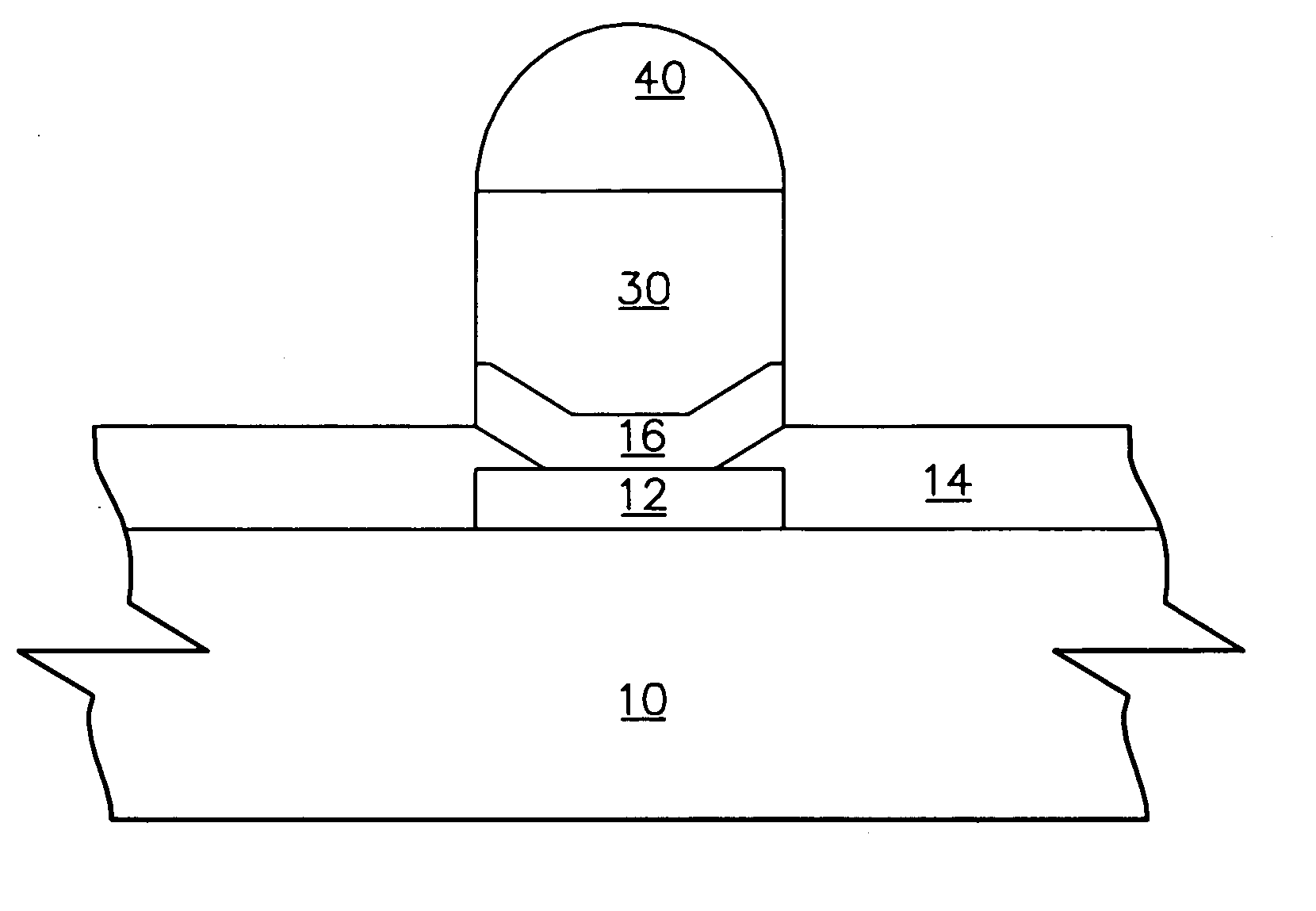
[0015] The present invention provides a method for increasing the height of a solder bump, and therefore improving the reliability of the solder bump. FIG. 2A to FIG. 2E are sectional views illustrating the steps of forming the solder bump according to one embodiment of the present invention. As shown in FIG. 2A, a semiconductor device 10 is provided with a conductive pad 12 formed on its surface. In the embodiment of the present invention, the semiconductor device 10 is a wafer, and the conductive pad 12 could be made of conductive material, such as aluminum or copper. A passivation layer 14 is formed on the semiconductor device 10, and the...


PUM

PropertyMeasurementUnit
melting pointaaaaaaaaaa
conductiveaaaaaaaaaa
melting pointaaaaaaaaaa

Abstract

A method of forming a solder bump and the associated structure is disclosed. A chip having a conductive pad is covered with a mask layer and exposing a potion of said conductive pad of said chip. Conductive material is then formed above the conductive pad not covered with said mask layer. After applying a flux material on the formed conductive material, a solder structure having a lower melting point than the conductive material is placed, and subsequently is reflowed at a temperature lower than the melting point of the conductive material. After removing the mask layer, the solder bump with increased height and reliability is thus attained.

Description

BACKGROUND OF THE INVENTION [0001] 1. Field of the Invention [0002] The present invention generally relates to the structure and the forming method of a solder bump, and more particularly to a solder bump with increased height and reliability. [0003] 2. Description of the Prior Art [0004] Flip chip technology has become one of the mainstreams to improve cost, reliability and productivity in the electronic packaging industry, relative to wire bonding technology. FIG. 1A to FIG. 1D are sectional views illustrating the steps of forming the solder bump using a conventional flip chip technology. Referring to FIG. 1A, a chip 100 is provided with conductive pad 102 formed on its surface, and then a passivation layer 104 is formed on the chip 100 to protect the chip 100. Thereafter, the passivation layer 104 is partially removed to expose the surface of the conductive pad 102, followed by covering the conductive pad 102 and the passivation layer 104 with under bump metallization (UBM) 106, ...

Claims


Application Information

Patent Timeline
Patent Type & Authority Applications(United States)
IPC IPC(8): H01L29/40H01L23/485H01L21/60
CPCH01L24/02H01L24/11H01L2224/0401H01L2224/1147H01L2224/13099H01L2924/01006H01L2924/01013H01L2924/01028H01L2924/01029H01L2924/0105H01L2924/01079H01L2924/01082H01L2924/014H01L2924/14H01L24/13H01L2924/01023H01L2924/01024H01L2924/01033H01L2224/13111H01L2924/00014H01L2924/0001H01L24/03H01L24/05
Inventor MIN-LUNG, HUANG
Owner ADVANCED SEMICON ENG INC
Why Eureka
Try Eureka