Liquid crystal display device

a display device and liquid crystal technology, applied in static indicating devices, instruments, non-linear optics, etc., can solve the problems of uneven display, alignment defect, and inability to efficiently apply electric field components parallel to the substrate surface to the liquid crystal layer, so as to reduce the frequency of alignment defects and prevent display failures. , good display quality

Inactive Publication Date: 2005-12-15
PANASONIC LIQUID CRYSTAL DISPLAY CO LTD +1
View PDF18 Cites 19 Cited by
  • Summary
  • Abstract
  • Description
  • Claims
  • Application Information

AI Technical Summary

Benefits of technology

[0027] An object of the present invention is to provide a liquid crystal display device having good display quality by solving the above problems in the art, specifically by decreasing the frequency of occurrence of alignment defects that result from the presence of steps of the storage capacitor portion Cstg formed in each pixel region and thereby preventing display failures such as a contrast reduction and display unevenness.
[0030] With the above configuration, the angles of steps in the storage capacitor portions with respect to the surface of an alignment film become gentle, whereby rubbing defects can be prevented from occurring in the vicinity of the storage capacitor portions. As a result, it becomes possible to provide a liquid crystal display device having good display quality in which the frequency of occurrence of display failures such as a contrast reduction and display unevenness are greatly reduced.
[0033] With the above two features, the angles of steps of the electrode films constituting the storage capacitor portions with respect to the surface of an alignment film become gentle, whereby rubbing defects can be prevented from occurring in the vicinity of the storage capacitor portions. As a result, it becomes possible to provide a liquid crystal display device having good display quality in which the frequency of occurrence of display failures such as a contrast reduction and display unevenness are greatly reduced.
[0036] The second object of the invention is to prevent the liquid crystal display device from display failures caused by the reduction of the voltage applied to its liquid crystal layer. This problem appears the liquid crystal display having such two kinds of conductive layers defined as first and second conductive layers as follows. The first and second conductive layers are formed above a main surface of one of substrates facing to the liquid crystal layer. The first conductive layer extends in first direction, and has a first voltage. The second conductive layer extends in second direction, and has a second voltage. Each of the first and second conductive layers has at least one portion therefrom in a different direction and joined thereto at a corner, and is covered with an insulating film.

Problems solved by technology

This is because it the interval between the electrodes is too short, electric lines of force are curved sharply and hence regions where electric field components parallel with the substrate surfaces are stronger than those perpendicular to the substrate surfaces are made larger, as a result of which the electric field components parallel with the substrate surfaces cannot be applied to the liquid crystal layer efficiently.
In those devices, the storage capacitor Cstg produces large steps in the pixel region and those steps may cause an alignment defect in a rubbing treatment.
As a result, what is called a domain occurs and causes display unevenness.
In particular, alignment defects of the above kind occur frequently in a case where the multilayered film structure that constitutes the storage capacitor portion Cstg has steps extending perpendicularly or approximately perpendicularly to the alignment direction (rubbing direction) of the alignment film.
This results in a problem that the contrast is lowered and display unevenness occurs, which means a marked reduction in image quality.

Method used


Image

  • Liquid crystal display device
  • Liquid crystal display device
  • Liquid crystal display device

Examples


first embodiment

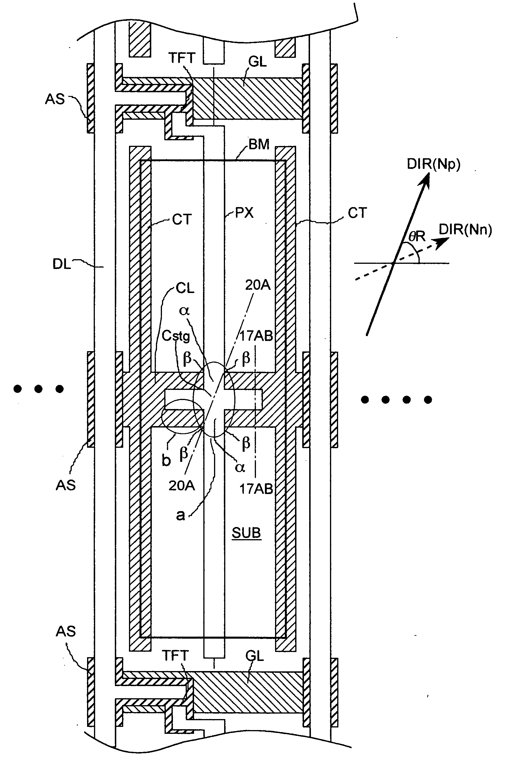
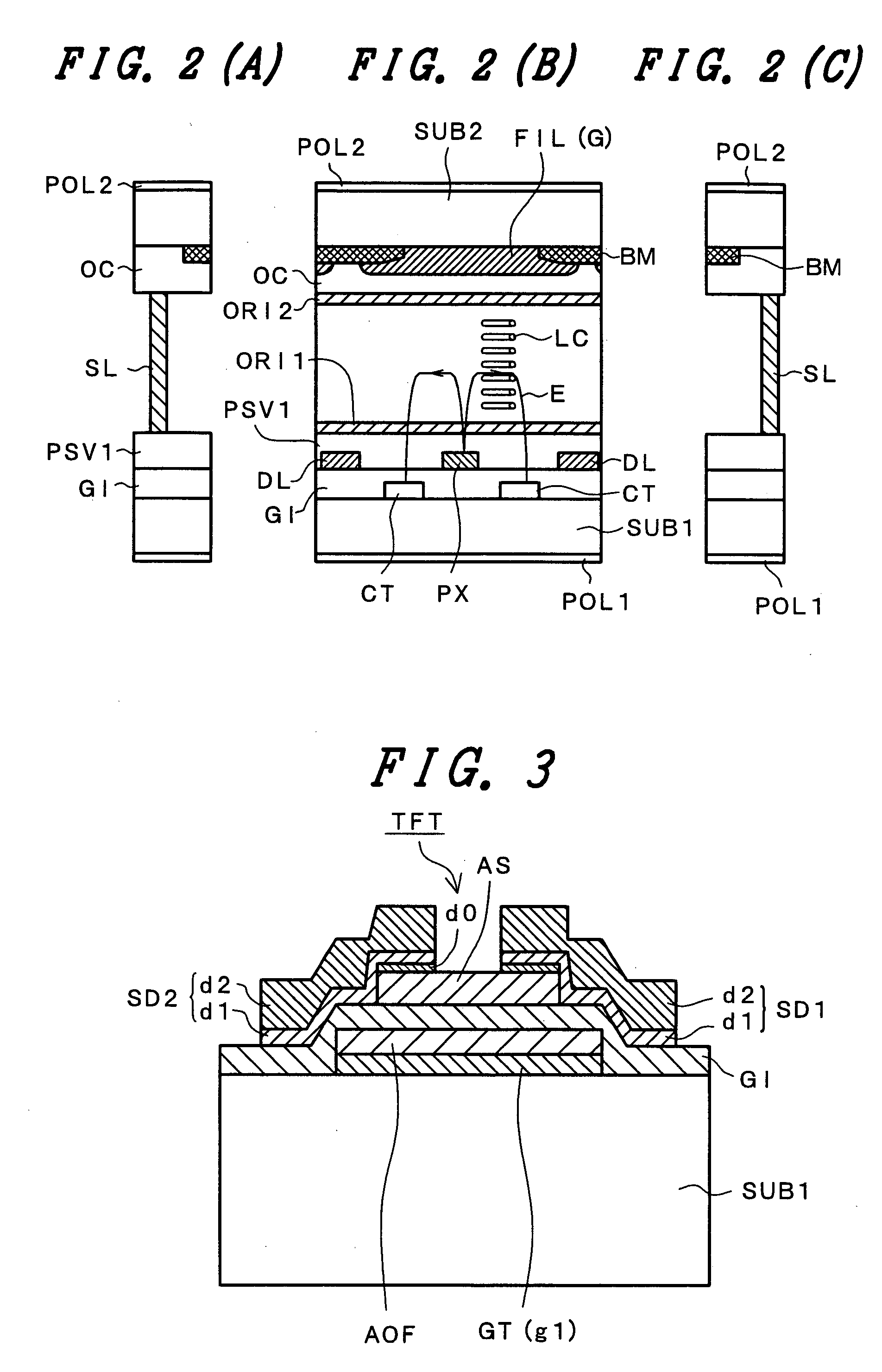
[0186]FIG. 16 is a schematic plan view of one pixel that is enclosed by a light shield film, that is, the main structure of a liquid crystal display device according to the invention.

[0187] Referring to FIG. 16, when a thin-film transistor TFT that is constituted of a video signal line DL, a scanning signal line GL, and an a-Si film is turned on, a signal voltage of the video signal line DL is transmitted to a pixel electrode PX and held by a storage capacitor portion Cstg that is composed of an counter voltage signal line CL and the pixel electrode PX (a dielectric film (insulating film) PS1 formed between the counter voltage signal line CL and the pixel electrode PX is not shown in FIG. 16).

[0188] A liquid crystal existing between the pixel electrode PX and the counter electrode CT is driven by the signal held by the storage capacitor portion Cstg.

[0189] The counter voltage signal line CL is located approximately at the center of the opening (pixel region) of a black matrix BM, ...

second embodiment

[0194]FIG. 18 is a schematic plan view of one pixel that is enclosed by a light shield film, that is, the main structure of a liquid crystal display device according to the invention.

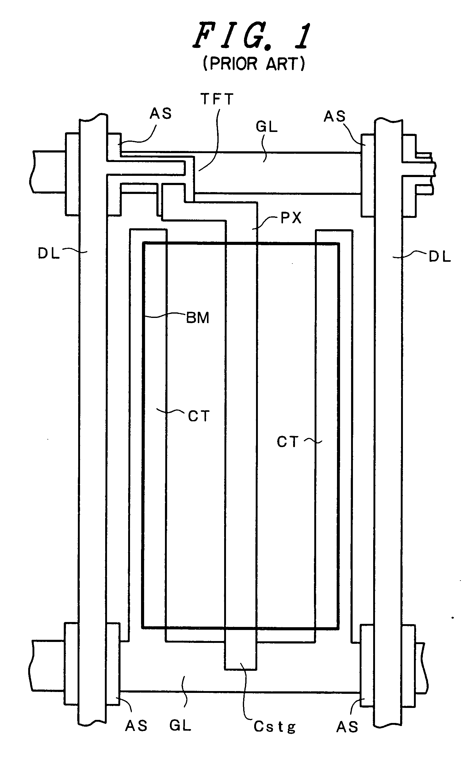
[0195] This embodiment has the same configuration as the first embodiment of FIG. 16 except that the numbers of comb-teeth portions of pixel electrodes PX and counter electrodes CT are increased. This configuration is suitable for a liquid crystal display device having a large screen.

third embodiment

[0196]FIG. 19 is a schematic plan view of one pixel that is enclosed by a light shield film, that is, the main structure of a liquid crystal display device according to the invention. FIGS. 20(A) and 20(B) are sectional views taken along line 20A-20A in FIG. 16 and line 20B-20B in FIG. 19, respectively.

[0197] In the first embodiment, as shown in FIG. 16, the portions of the pixel electrode PX that are connected to the storage capacitor Cstg cross the level differences at the peripheries of the counter voltage signal line CL.

[0198] In the portions indicated by symbol a in FIG. 16 (also indicated by symbol a in FIG. 20(A)) of the pixel electrode PX at the crossing portions, the inclination angle is approximately equal to the inclination angle θCL of the gently sloped peripheries the counter voltage signal line CL (lower layer). Therefore, even the probability that a large level difference causes a rubbing defect is low.

[0199] However, in the peripheral portions (indicated by symbol ...


PUM

PropertyMeasurementUnit
thicknessaaaaaaaaaa
thicknessaaaaaaaaaa
widthsaaaaaaaaaa

Abstract

A display device includes a first substrate having formed thereon a plurality of video signal lines and a plurality of gate signal lines, a plurality of pixel electrodes, a plurality of thin film transistors, and a plurality of pixels. Each pixel includes a pixel electrode of the plurality of pixel electrodes and a thin film transistor of the plurality of thin film transistors. The thin film transistor includes a semiconductor layer, a drain electrode electrically connected to a drain signal line, and a source electrode electrically connected to the pixel electrode. The semiconductor layer has an outline so that a nearest portion to a center of the pixel is positioned under the source electrode in plan view.

Description

CROSS REFERENCE TO RELATED APPLICATION [0001] This is a continuation of U.S. application Ser. No. 10 / 779,794, filed Feb. 18, 2004, which is a continuation of U.S. application Ser. No. 10 / 400,686, filed Mar. 28, 2003, now U.S. Pat. No. 6,697,142, which is a continuation of U.S. application Ser. No. 10 / 038,599, filed Jan. 8, 2002, now U.S. Pat. No. 6,545,736, which is a continuation of U.S. application Ser. No. 09 / 234,494, filed Jan. 21, 1999, now U.S. Pat. No. 6,341,003, the subject matter of which is incorporated by reference herein.BACKGROUND OF THE INVENTION [0002] 1. Field of the Invention [0003] The present invention relates to a liquid crystal display device and, more specifically, to a liquid crystal display device in which a pair of insulating substrates are opposed to each other via a predetermined gap that is maintained by spacers, a liquid crystal composition (a liquid crystal molecule) is held in the gap, and a storage capacitor portion is formed in each pixel region. [00...

Claims


Application Information

Patent Timeline
Patent Type & Authority Applications(United States)
IPC IPC(8): G02F1/1337G02F1/1343G02F1/1362
CPCG02F1/133784G02F1/134363G02F1/1345G02F1/13452G09G2300/0434G02F2001/133776G02F2201/128G09G3/3611G09G2300/0426G02F1/136213G02F1/133776G02F1/1337
Inventor ASHIZAWA, KEIICHIROHIKIBA, MASAYUKIOHTA, MASUYUKI
Owner PANASONIC LIQUID CRYSTAL DISPLAY CO LTD
Why Eureka
Try Eureka