Circuit for PLL-based at-speed scan testing

a technology of at-speed scan and circuit, applied in the direction of transmission monitoring, line-transmission details, instruments, etc., can solve the problems of multiple clock domains and difficult simultaneous testing of different domains using scan test vectors, and achieve the effect of ics employing multiple clock domains

Inactive Publication Date: 2005-12-15
AVAGO TECH INT SALES PTE LTD
View PDF3 Cites 20 Cited by
  • Summary
  • Abstract
  • Description
  • Claims
  • Application Information

AI Technical Summary

Benefits of technology

[0019]FIG. 8 is a block schematic diagram of an example ch

Problems solved by technology

If two or more clock domains in the IC communicate with one another, then the simultaneous testing of the different domains using scan test vectors may be difficult to achieve, sinc

Method used


Image

  • Circuit for PLL-based at-speed scan testing
  • Circuit for PLL-based at-speed scan testing
  • Circuit for PLL-based at-speed scan testing

Examples


Embodiment Construction

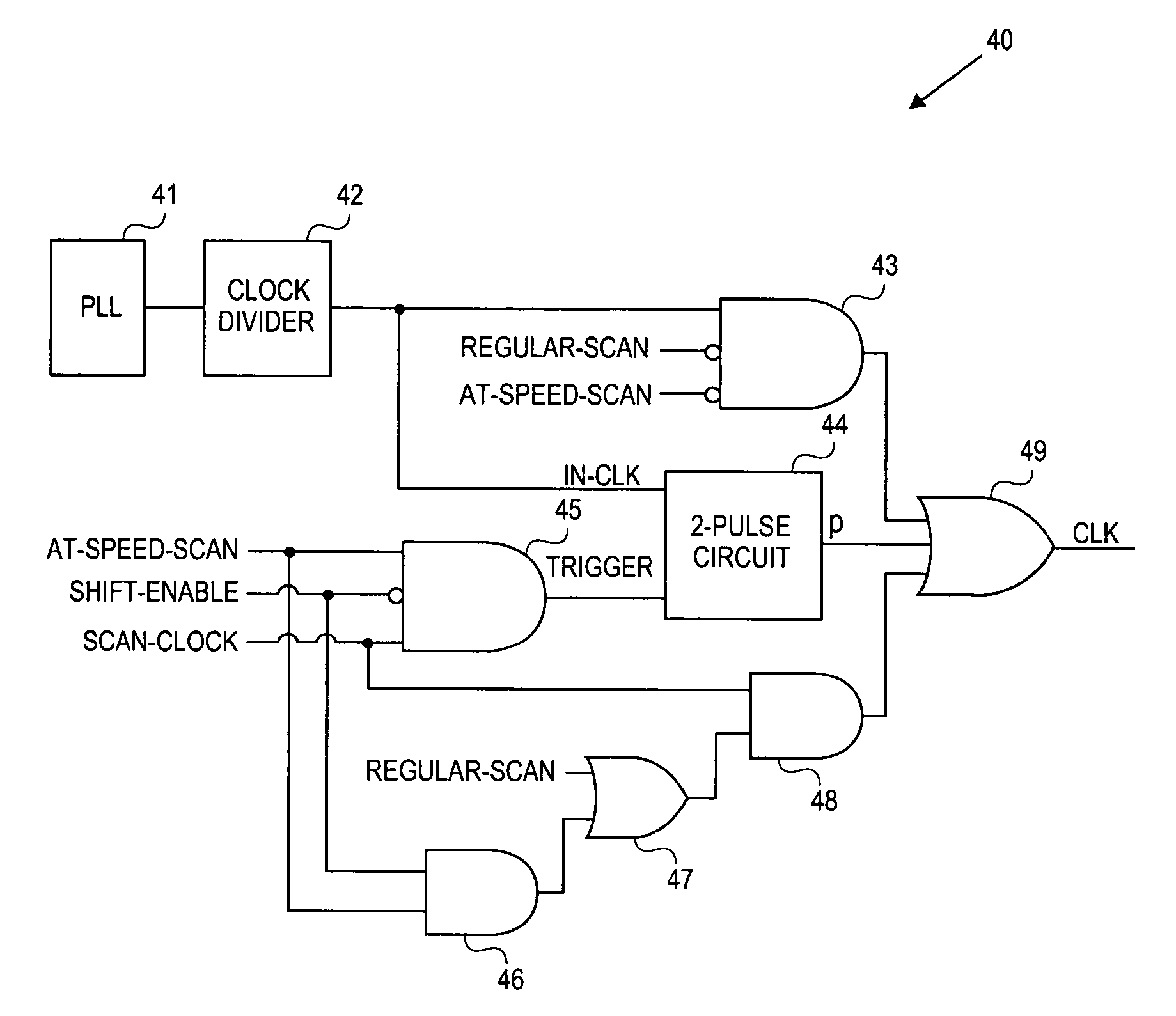
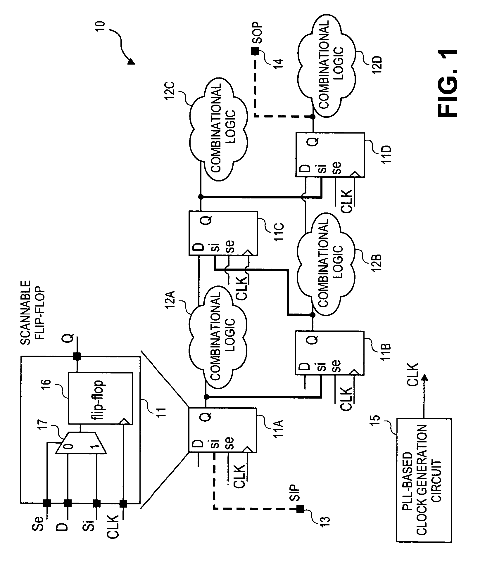
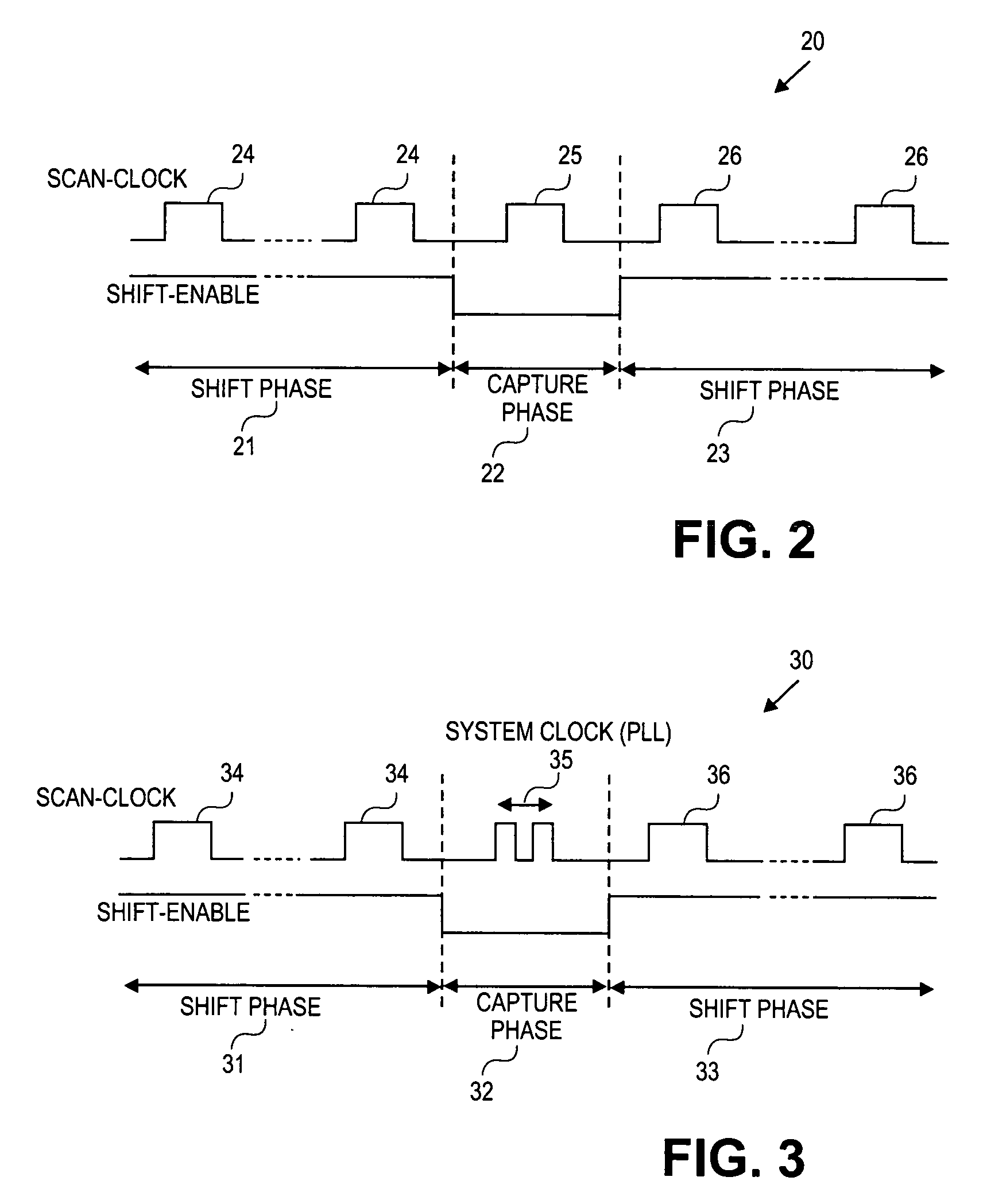
[0020] The embodiments of the present invention may be practiced in a variety of settings that scan testing is used. It may be used in integrated circuits having single clock domains or multiple clock domains. Generally, it is understood that some form of software tool, such as an Automatic Test Pattern Generation (ATPG) tool, is used to generate the test vectors. These test vectors include the test signal inputs and expected response from the integrated circuit. These test vectors are typically applied to the integrated circuit using Automatic Test Equipment (ATE). Furthermore, much of the discussion centers on at-speed scan testing, since this technique involves more complexity. However, regular scan techniques may be employed as well for scan testing an integrated circuit. Additionally, the description below discusses operations of various circuitry using signal states, such as activating on high. It is to be noted that equivalent circuits may be designed with other states perfor...


PUM


Abstract

A scheme for PLL-based at-speed scan testing in which a clock generation circuit is used to generate different clock signals to scannable flip-flops of an integrated circuit. When the integrated circuit is under at-speed scan test mode of operation, the clock generation circuit receives a scan-clock signal to scan in a test vector to the scannable flip-flops during an input shift phase when shifting is enabled and to scan out a resultant vector from the scannable flip-flops during an output shift phase when shifting is also enabled. However, when shifting is not enabled during a capture phase between the two shift phases, the scan-clock signal triggers a 2-pulse circuit to release two pulses during the capture phase of at-speed scan testing. The two pulses from the 2-pulse circuit are based on an internal PLL-based clock signal. The clock generation circuit may be utilized in single or multiple clock domain systems. In a multiple clock domain environment, separate scan-clock signals may be sent to individual clock domains within an integrated circuit and only the domain to be acted on by a test vector has its respective scan-clock pulsed during the capture phase.

Description

BACKGROUND OF THE INVENTION [0001] 1. Technical Field of the Invention [0002] The embodiments of the invention relate to scan testing of integrated circuits and, more particularly, to a PLL-based at-speed scan testing scheme. [0003] 2. Description of Related Art [0004] Generally, integrated circuits are tested after manufacture to ensure that the integrated circuits are not operationally defective. One testing technique employs the use of scanning vectors, in which a particular test vector is shifted into an integrated circuit (IC) prior to running the IC's combinational logic in its normal mode. A resultant output vector is then read to determine the response of the IC to the scanned in test vector. For high complexity ICs, one popular technique is the use of scannable flip-flops in the IC for scan testing. Some ICs employ full scan techniques, in which all of the flip-flops in the IC design are made scannable. Scannable flip-flops allow a test vector to be shifted in to load the f...

Claims


Application Information

Patent Timeline
IPC IPC(8): G01R31/3185H04B3/46
CPCG01R31/318541G01R31/31858G01R31/318555
Inventor KONUK, HALUK
Owner AVAGO TECH INT SALES PTE LTD
Why Eureka
Try Eureka