Image processing device, image processing method and image processing program

a technology of image processing and image processing method, applied in the field of image processing device, image processing method and image processing program, can solve the problems of spatial resolution degrade, essentially decreasing resolution, and pixel count for a specified color

Inactive Publication Date: 2005-12-15
CANON KK
View PDF5 Cites 102 Cited by
  • Summary
  • Abstract
  • Description
  • Claims
  • Application Information

AI Technical Summary

Problems solved by technology

However, with the aforementioned RGB color Bayer pattern, for example, simply interpolating results in the resolution essentially decreasing, because G has only one half of all the pixels and R and B each have only one fourth of all the pixels.
However, the demosaicing processes proposed therein are based on spatial interpolation of same color pixels, and therefore when the number of colors in the color filter is increased, the pixel count for a specified color decreases and spatial resolution degrades and becomes a problem.
Further, even with a random color filter array, similar problems can occur because regions wherein pixels of the same color become locally non-dense occur.
Further, the discrepancy of the color permeability characteristics, based on manufacturing error of the color filter array between the pixels of the same pixel color, is manifested as noise.

Method used


Image

  • Image processing device, image processing method and image processing program
  • Image processing device, image processing method and image processing program
  • Image processing device, image processing method and image processing program

Examples


first embodiment

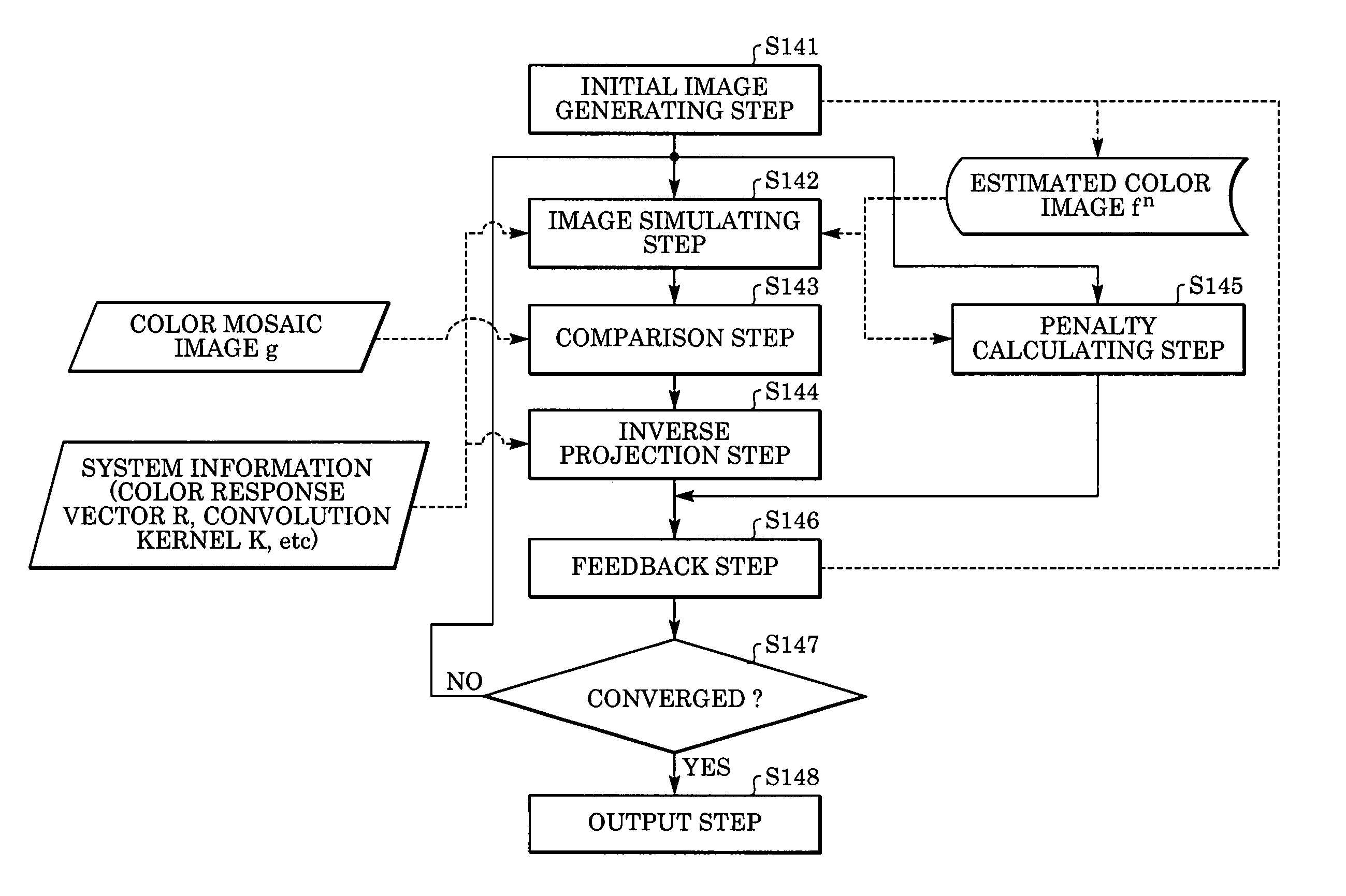
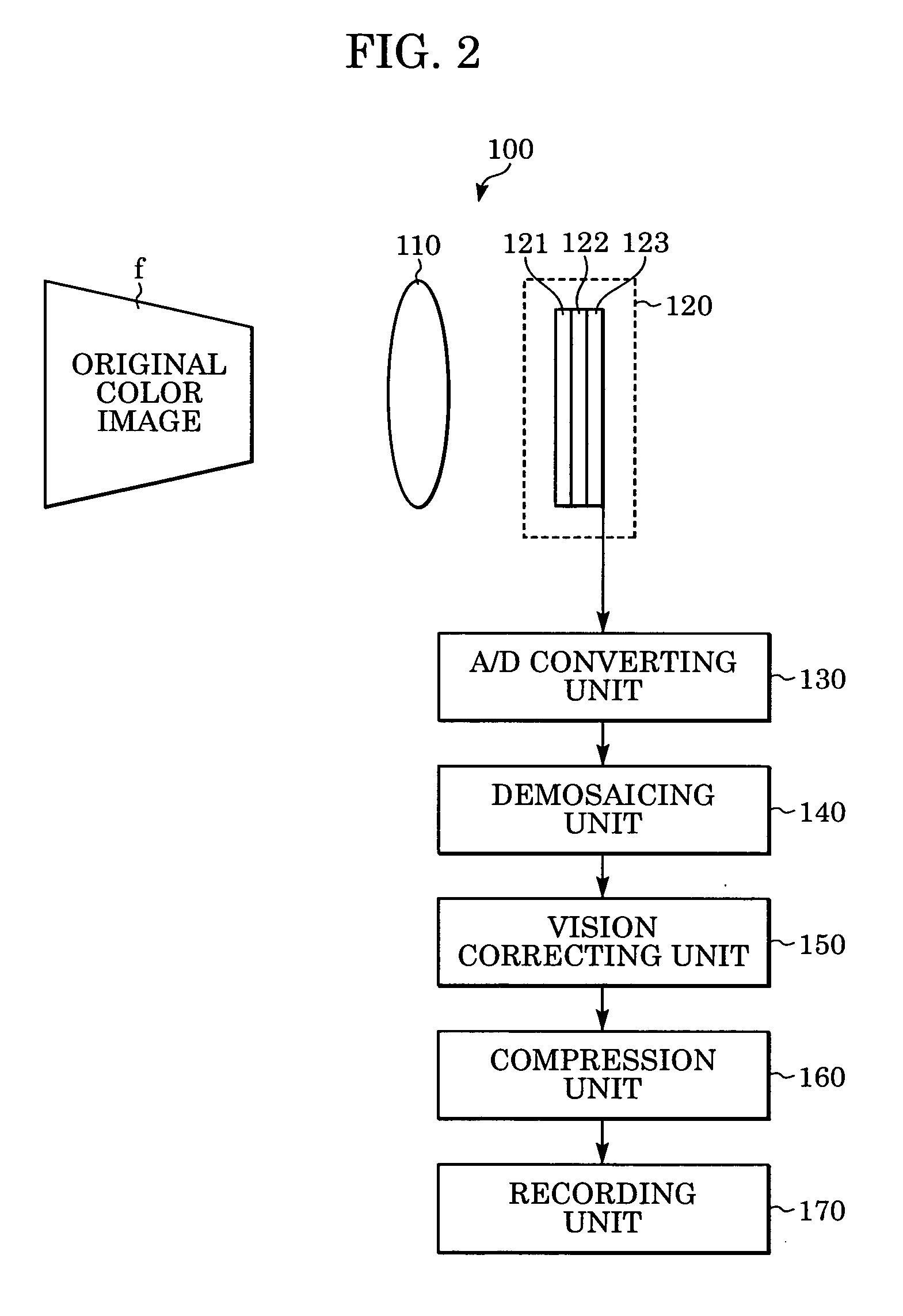
[0093] The image processing device and a color imaging device (digital camera) 100 in which the image processing device is loaded according to the first embodiment of the present invention are described next.

[0094] In FIG. 2, the color imaging device 100 includes an imaging optical system 110, a single-CCD color image sensor 120, an A / D (analog-to-digital) converting unit 130, a demosaicing unit 140, a vision correcting unit 150, a compression unit 160, and a recording unit 170. The original color image f illustrated in FIG. 2 hypothetically illustrates the field, and is not a component of the color imaging device 100, but is shown in FIG. 2 for the purpose of explanation.

[0095] The photographed original color image f is formed upon the single-CCD color image sensor 120 via the imaging optical system 110. Here, the single-CCD color image sensor 120 includes a color filter array 122 on the front side of a solid-state image sensor 123, and the image which is imaged upon the solid-st...

second embodiment

[0130] The demosaicing process described in the first embodiment is an appropriate method in the case in which the noise generated in the solid state image sensor 123 and the A / D converting unit 130 is modeled, assumed to follow a Gaussian distribution. This is applicable to the case with noise wherein the dark current of the solid-state image sensor 123 is dominant.

[0131] On the other hand, with the combination of a solid-state image sensor with high sensitivity and low noise and an A / D converting unit, the output of the A / D converting nears the photon count, the quantum Poisson noise becomes the dominant noise. In the present embodiment, an appropriate demosaicing process including noise reduction will be described as to a color imaging device that has a high sensitivity and low noise solid-state image sensor.

[0132] The demosaicing process of the present embodiment performs processing according to the same flowchart as in the first embodiment; however, the operations of the comp...

third embodiment

[0141] As an application differing from the first and second embodiments of the present invention, a color imaging device with a color filter array such as that illustrated in FIG. 4 will be described. The configuration of the color imaging device of the present embodiment is similar to the color imaging device 100 described in the first embodiment, but the color pattern of the color filter array 122 differs from the first embodiment.

[0142] The color filter array 122 of the present embodiment has, other than the normal RGB color filters R, G, B, a G filter DG with low transmission, and is a four-color color filter with R, G, B, and DG. The color response vector in the RGB color space of the pixels corresponding to the various color filters shall be (100)·(010)·(001)·(00.20)(42)

[0143] Further, the solid-state image sensor 123 and the A / D converting unit 130 attain output saturation (luminescence saturation) even if the light is cast into the pixels with an intensity greater than 1,...


PUM


Abstract

An image processing device generates an output image as a color image wherein each pixel has color information, using a first image as a sparsely color sampled image wherein each pixel has monochromatic information obtained by an image sensor which has multiple pixels each photoelectrically converting light of a plurality of colors. The device includes: a simulation unit for generating a second image as an estimated image of the sparsely color sampled image; a comparison unit for comparing the second image with the first image, and generating first information thereof; a converting unit for converting the first information into second information corresponding to the color image; a penalty computing unit for computing the correction amount of the input image; and a correction unit for generating a third image by correcting the input image based on the second information and the correcting amount; this third image being used as an output image.

Description

BACKGROUND OF THE INVENTION [0001] 1. Field of the Invention [0002] The present invention relates to an image processing device, method, and program, for generating a color image from a sparsely color sampled image which is acquired by using a single-chip color image sensor, and further relates to an image processing device, method, and program, for performing a demosaicing process including processing such as noise reduction, optical low-pass filter compensation and pixel drop-out processing. [0003] 2. Description of the Related Art [0004] Hitherto, single-CCD (charge-coupled device) color image sensors have been widely used in color imaging devices such as digital cameras and compact video cameras. A single-CCD color image sensor includes, on the front face of a solid-state image sensor, a color filter array in which color transmission properties that differ for each pixel are provided in a specified array or a random array. For example, a color filter array such as illustrated in...

Claims


Application Information

Patent Timeline
Patent Type & Authority Applications(United States)
IPC IPC(8): H04N1/48H04N1/60H04N1/64G06T1/00H04N9/04H04N9/07H04N9/083
CPCH04N1/648H04N3/155H04N9/045G06T2207/10024G06T5/002G06T5/003G06T5/20H04N2209/046H04N23/843H04N25/133H04N25/135H04N25/134
Inventor SAWADA, YASUHIRO
Owner CANON KK
Why Eureka
Try Eureka