Electronic assembly having an indium wetting layer on a thermally conductive body

Active Publication Date: 2005-12-22
INTEL CORP
View PDF6 Cites 53 Cited by
  • Summary
  • Abstract
  • Description
  • Claims
  • Application Information

AI Technical Summary

Problems solved by technology

Such a chip or die may have solder bump contacts on the integrated circuit.

Method used


Image

  • Electronic assembly having an indium wetting layer on a thermally conductive body
  • Electronic assembly having an indium wetting layer on a thermally conductive body
  • Electronic assembly having an indium wetting layer on a thermally conductive body

Examples


Embodiment Construction

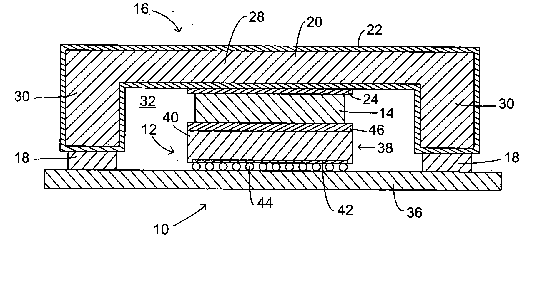
[0009] U.S. Pat. No. 6,504,242 describes an electronic assembly including a die and a heat spreader. The heat spreader has a nickel layer formed thereon, and a gold wetting layer on the nickel layer. The nickel layer acts as a diffusion barrier. The purpose of the gold layer is to serve as a wetting layer for an indium preform positioned between the heat spreader and the die. The stack is heated and cooled to “solder” the indium to the gold. During this operation an intermetallic layer including indium and gold (AuIn2) is typically also formed.

[0010] Applicants have observed that thermal degradation of such an electronic assembly as described in U.S. Pat. No. 6,504,242 may occur. The thermal degradation may result in failures due to crack propagation between the indium-gold intermetallic layer and the indium layer.

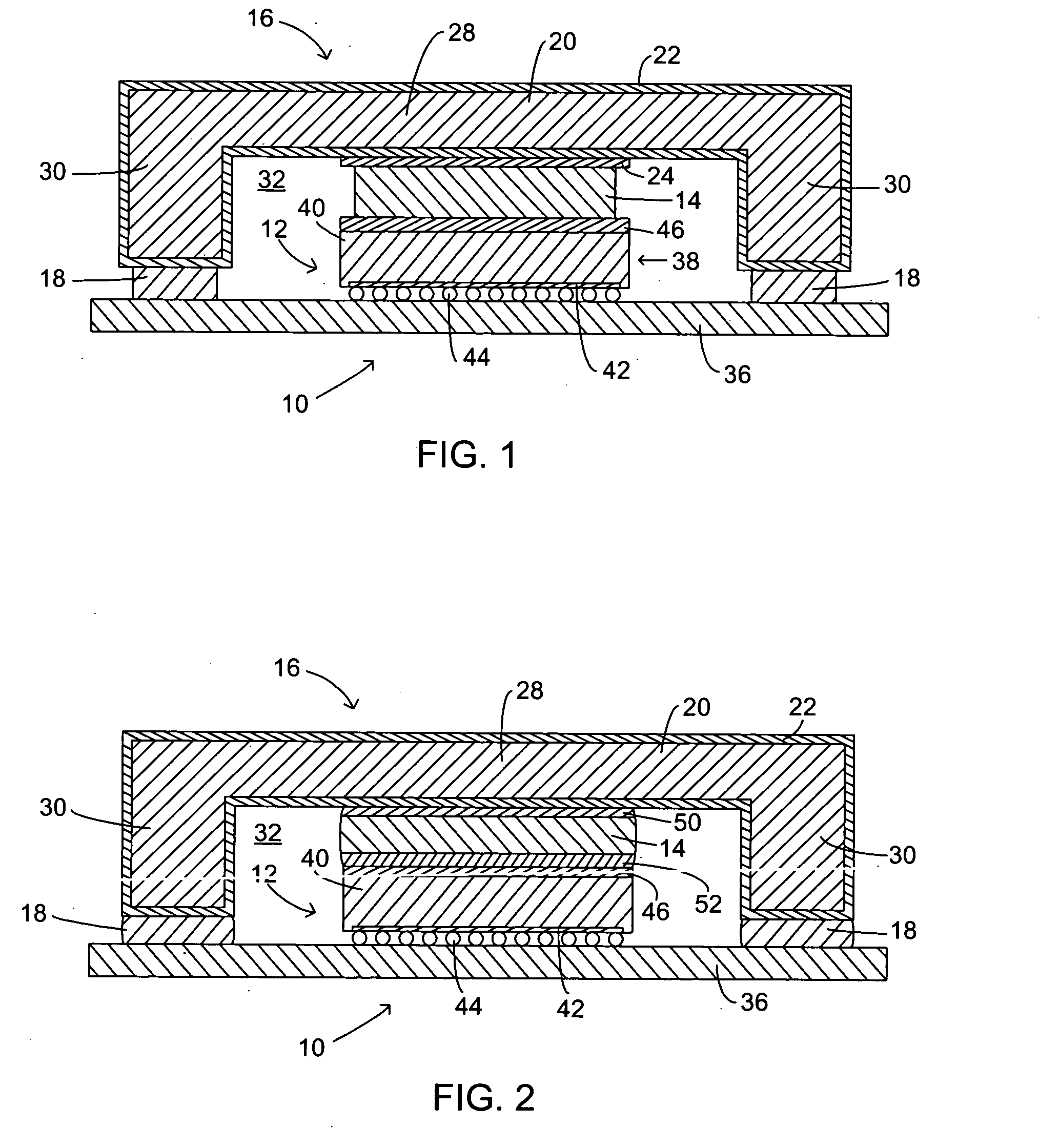
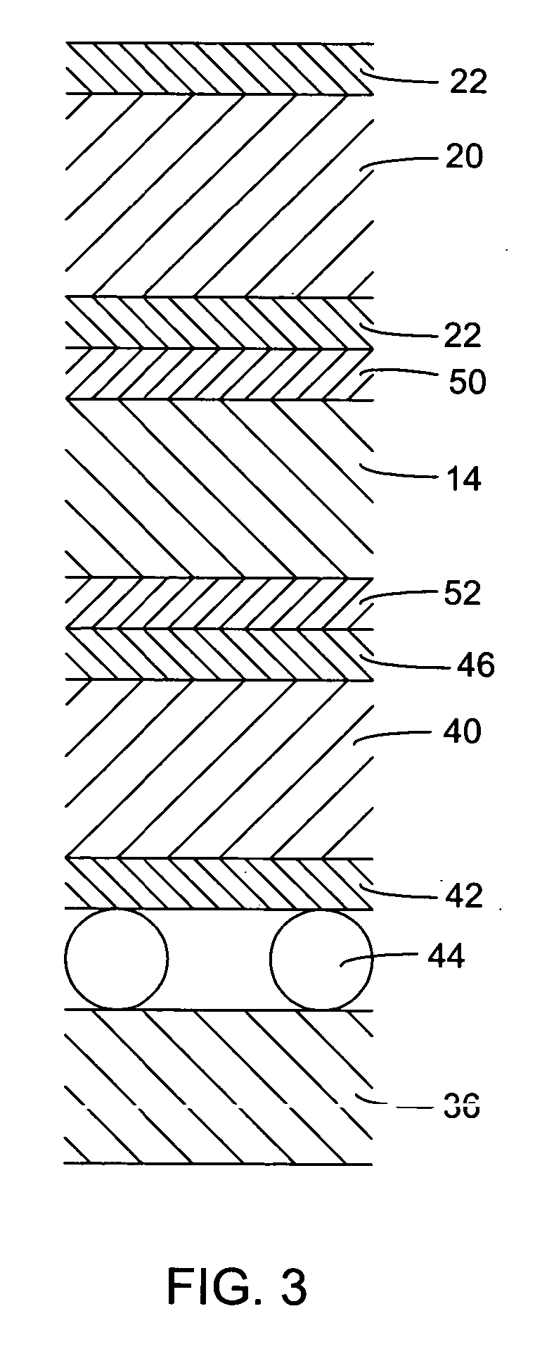
[0011]FIG. 1 of the accompanying drawings illustrates components of an electronic assembly 10 according to an embodiment of the present invention, before being finally a...


PUM

PropertyMeasurementUnit
thicknessaaaaaaaaaa
thicknessaaaaaaaaaa
thicknessaaaaaaaaaa

Abstract

Embodiments include electronic packages and methods for forming electronic packages. One method includes providing a die and a thermal interface material on the die. A metal body is adapted to fit over the die. A wetting layer of a material comprising indium is formed on the metal body. The thermal interface material on the die is brought into contact with the wetting layer of material comprising indium. The thermal interface material is heated to form a bond between the thermal interface material and the wetting layer so that the thermal interface material is coupled to the metal body, and to form a bond between the thermal interface material and the die so that the thermal interface material is coupled to the die.

Description

TECHNICAL FIELD [0001] Embodiments of the present invention relate generally to electronics packaging. More particularly, certain embodiments of the present invention relate to an electronic assembly including a semiconductor die which is thermally coupled through an interface material to a thermally conductive body to dissipate heat, and to manufacturing methods thereof. RELATED ART [0002] Integrated circuits are generally formed on semiconductor wafers formed from materials such as silicon. The semiconductor wafers are processed to form various electronic devices thereon. The wafers are diced into semiconductor chips, which may then be attached to a package substrate. Such a chip or die may have solder bump contacts on the integrated circuit. The solder bump contacts extend downward onto contact pads of a package substrate, and are typically attached in a thermal reflow process. Electronic signals may be provided through the solder bump contacts to and from the integrated circuit....

Claims


Application Information

Patent Timeline
Patent Type & Authority Applications(United States)
IPC IPC(8): H01L23/10H01L23/34H01L23/433
CPCH01L23/10H01L2224/0401H01L23/3736H01L23/433H01L24/32H01L2224/04026H01L2224/16225H01L2224/73253H01L2924/01005H01L2924/01013H01L2924/01029H01L2924/01049H01L2924/0105H01L2924/01074H01L2924/01078H01L2924/01079H01L2924/01327H01L2924/14H01L2924/16152H01L2924/01006H01L2924/01023H01L23/3735H01L2924/3512H01L2924/00H01L2224/2612
Inventor HUA, FAYFITZGERALD, THOMAS J.DEPPISCH, CARL L.CHRYSLER, GREGORY M.
Owner INTEL CORP
Why Eureka
Try Eureka