Semiconductor device module with flip chip devices on a common lead frame

a technology of semiconductor devices and lead frames, which is applied in the direction of semiconductor devices, semiconductor/solid-state device details, electrical apparatus, etc., can solve the problems of thermal increase, part interference with the operation of microprocessors, etc., and achieve the effect of improving thermal management and superior thermal managemen

Active Publication Date: 2005-12-22
INFINEON TECH AMERICAS CORP
View PDF21 Cites 40 Cited by
  • Summary
  • Abstract
  • Description
  • Claims
  • Application Information

AI Technical Summary

Benefits of technology

[0013] Second, it is an object of the present invention to provide such a planar arrangement, while eliminating the need to provide wire bonding to effect connections between the various die in the common housing.
[0014] Third, it is an object of the present invention to provide a planar arrangement of die in a common housing that exhibits superior thermal management over conventional planar arrangements of die and over stacked or superimposed arrangements of die.
[0015] Therefore, the invention comprises a plurality of flip chip devices arranged on a common lead frame or other circuit substrate, the arrangement being in substantially planar fashion without any stacking or superimposing of one flip chip device over any other flip chip device. The connections between the flip chip devices are made without any wire bonding. The connection between at least some of the flip chip devices provides improved thermal management over that available with conventional planar arrangements of die or stacked or superimposed arrangements of die in a common housing.

Problems solved by technology

If the part is near other components, such as microprocessors, the part can interfere with the operation of the microprocessor.
However, such an approach may involve increases in the thermal effects the operation of one die would have on the other die stacked or superimposed on it over the planar arrangement approach.

Method used


Image

  • Semiconductor device module with flip chip devices on a common lead frame
  • Semiconductor device module with flip chip devices on a common lead frame
  • Semiconductor device module with flip chip devices on a common lead frame

Examples


Embodiment Construction

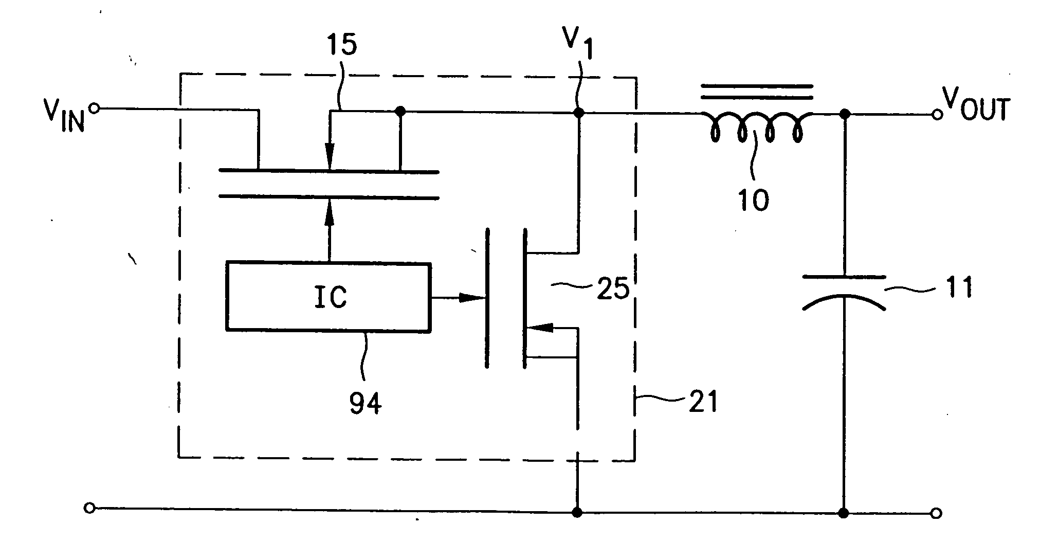
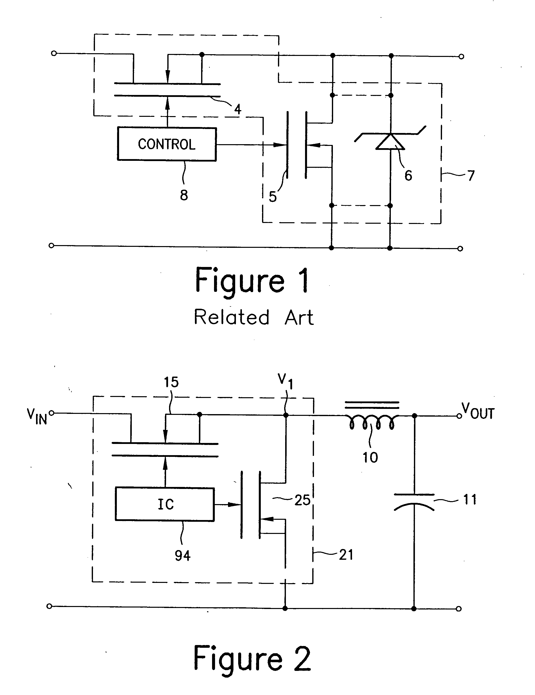
[0024]FIG. 2 shows a circuit diagram of a buck converter circuit including a MOSFET of top drain construction 15, a synchronous MOSFET 25, the synchronous MOSFET 25 being of a DirectFET™ type, a flip chip type IC 94, controlling MOSFETs 15 and 25 in a PWM mode to obtain a constant output DC voltage, an inductor 10 and a capacitor 11. The buck converter circuit, sometimes known as a step down converter, is commonly used to reduce voltages. Therefore, the input voltage VIN is greater than the output voltage VOUT. The MOSFET die 15, the MOSFET die 25, and the IC die 94 are arranged in a common housing 21. The die 15, 25, 94 are arranged in a planar fashion on a lead frame 20 or other substrate which is both thermally and electrically conductive.

[0025] The thermal conductivity of the lead frame or other substrate is needed to assure effective transmission of heat away from die 15, 25, 94 and toward one or more heatsinks (not shown) below the lead frame or other substrate. The electrica...


PUM


Abstract

The semiconductor portion of a circuit includes a plurality of flip chip devices which are arranged in a planar fashion in a common housing. The plurality of flip chip devices are connected to each other without wire bonding. The common housing includes a packaging structure, the packaging structure including a connective portion and at least one web portion, which aids in the thermal management of the heat emitted by the plurality of flip chip devices and which connects the flip chip devices to each other. Passive devices in the circuit may also be arranged in a planar fashion in the common housing.

Description

CROSS-REFERENCE TO RELATED APPLICATION [0001] This application claims the benefit of U.S. Provisional Application No. 60 / 576,703, filed on Jun. 3, 2004, the entirety of the contents of which is hereby incorporated by reference herein.BACKGROUND OF THE INVENTION [0002] 1. Field of the Invention [0003] The present invention relates to a module comprising flip chip devices forming at least the semiconductor portion of a circuit. [0004] 2. Description of the Related Art [0005] Numerous types of electrical circuits, such as DC to DC converters, synchronous converters, and the like, require a number of semiconductor components such as MOSFETs and ICs. Such circuit components can be found in portable electronics apparatus and the support components are commonly separately housed and mounted individually on a support board. The separately housed parts take up board space and each part generates heat. If the part is near other components, such as microprocessors, the part can interfere with ...

Claims


Application Information

Patent Timeline
Patent Type & Authority Applications(United States)
IPC IPC(8): H01L23/34H01L23/48H01L23/538H01L25/16
CPCH01L23/5385H01L25/162H01L2224/73253H01L2224/16225H01L2924/1306H01L24/01H01L2924/13091H01L2924/12032H01L2224/32225H01L2924/00H01L2924/14
Inventor SCHAFFER, CHRISTOPHER P.CHEAH, CHUANHU, KEVIN
Owner INFINEON TECH AMERICAS CORP
Why Eureka
Try Eureka