Circuit apparatus and method of manufacturing the same

a technology of circuit apparatus and heat radiation characteristic, which is applied in the direction of insulating substrate metal adhesion improvement, printed resistor incorporation, and association of printed circuit non-printed electric components, etc., can solve the problems of high requirements for packaging itself, difficult to achieve portable electronic equipment and the like that are reduced in size, profile, weight, and other issues, to achieve the effect of improving the heat radiation characteristic and improving the adhesiveness

Inactive Publication Date: 2005-12-29
SANYO ELECTRIC CO LTD
View PDF5 Cites 18 Cited by
  • Summary
  • Abstract
  • Description
  • Claims
  • Application Information

AI Technical Summary

Benefits of technology

[0013] The present invention has been achieved in view of the foregoing circumstances. It is thus an object of the present invention to provide a technology for improving the adhesiveness between the boa

Problems solved by technology

Consequently, while the LSI chips of higher integration have grown in the number of I/Os, miniaturization has been highly required of the packages themselves.
Hei 8-162486, however, it has been difficult to achieve portable electronic equipment and the like that are reduced in size, profile, and weight up to the levels desired at present.
The improvement to the heat radiation characteristic has also been limited.
In the techniques of forming a layer containing passive elements composed of resistor parts, capacitor parts, and/or patterned wiring parts as disclosed in Japanese Patent Laid-Open

Method used


Image

  • Circuit apparatus and method of manufacturing the same
  • Circuit apparatus and method of manufacturing the same
  • Circuit apparatus and method of manufacturing the same

Examples


Embodiment Construction

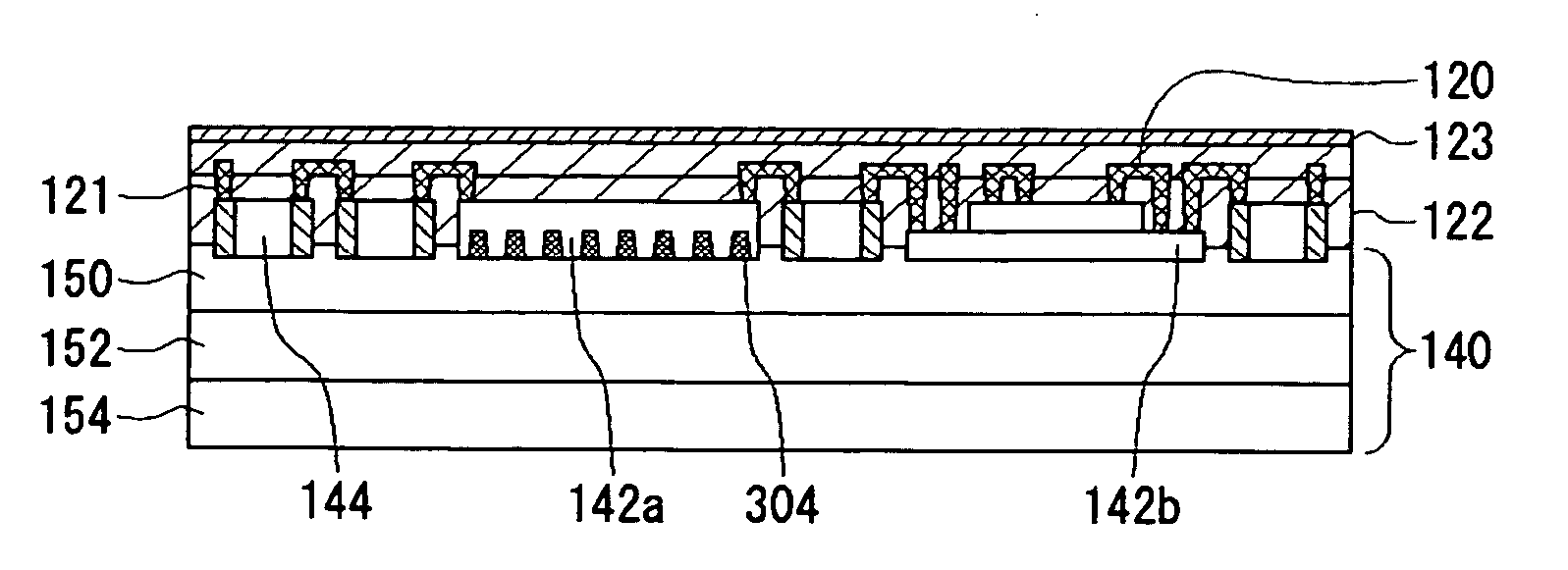
[0040] Hereinafter, an embodiment of the present invention will be described with reference to the drawings. Incidentally, in any of the drawings, identical components will be designated by like reference numerals. Description thereof will be omitted as appropriate. As employed herein, an “upward” direction is a concept to be determined by the order of lamination of films. The direction in which a film laminated later lies as viewed from a film laminated before shall be defined as “upward.”

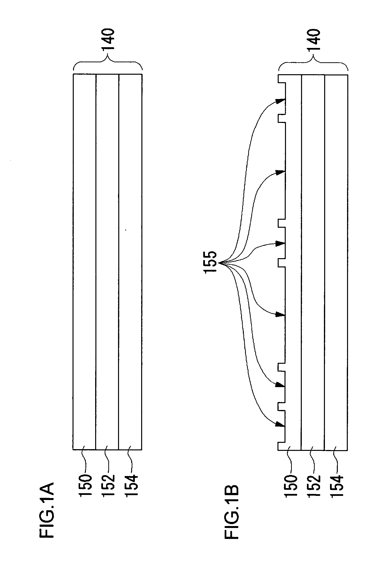
[0041]FIGS. 1A and 1B are sectional views for showing the steps of manufacturing a substrate to be used for a circuit apparatus according to the present embodiment. The substrate 140 may be made of a clad material that includes a metal having a coefficient of thermal expansion of 0.5 to 5.0×10⁻⁶ / K and a metal having a thermal conductivity of 200 to 500 W / mK in combination. Fe, Ni, and Co alloys are suitable for the metal having a coefficient of thermal expansion of 0.5 to 5.0×10⁻⁶ / K. Other metals ...


PUM


Abstract

Circuit elements including a plurality of semiconductor devices and passive elements embedded in an insulating resin film are formed on a metal substrate having a surface roughness Ra of 0.3 to 10 μm. This produces an anchoring effect occurs between the substrate and the insulating film, thereby improving the adhesiveness between the substrate and the insulating resin film.

Description

BACKGROUND OF THE INVENTION [0001] 1. Field of the Invention [0002] The invention relates to a circuit apparatus and a method of manufacturing the same. [0003] 2. Description of the Related Art [0004] Portable electronics equipment including cellular phones, PDAs, DVCs, and DSCs has been advancing at increasingly fast speed. Under the circumstances, miniaturization and weight saving have become essential in order for these products to be accepted in the market. To achieve this, system LSIs of higher integration have been sought after. Meanwhile, enhanced usability and convenience have been desired of such electronics equipment, and functional and performance sophistication has been required of the LSIs to be used for the equipment. Consequently, while the LSI chips of higher integration have grown in the number of I / Os, miniaturization has been highly required of the packages themselves. For the sake of satisfying both the requirements, there has been a strong demand to develop a se...

Claims


Application Information

Patent Timeline
IPC IPC(8): H01L21/02H01L21/3205H01L21/4763H01L21/82H01L23/14H01L23/538H01L27/01H01L27/10H01L29/739H05K1/05H05K1/16H05K1/18H05K3/38H05K3/46
CPCH01L23/142H01L2924/014H01L24/18H01L24/82H01L27/013H01L27/016H01L28/20H01L28/40H01L2224/18H01L2224/32145H01L2224/48091H01L2924/01013H01L2924/01027H01L2924/01029H01L2924/01073H01L2924/01074H01L2924/01078H01L2924/01079H01L2924/01088H01L2924/10158H01L2924/14H01L2924/15311H01L2924/19041H01L2924/19043H01L2924/19105H05K1/056H05K1/162H05K1/167H05K1/185H05K3/382H05K3/4644H05K2201/0187H05K2201/0338H05K2201/09745H01L23/5389H01L2924/01076H01L24/48H01L2924/01005H01L2924/01006H01L2924/01019H01L2924/01024H01L2924/01033H01L2924/01047H01L2924/00014H01L2224/451H01L2924/12042H01L24/45H01L2224/24137H01L2224/24145H01L2224/24195H01L2224/73267H01L2224/12105H01L2224/32245H01L2224/8203H01L2924/181H01L2924/3511H01L2224/04105H01L2224/92244H01L24/24H01L24/19H01L2924/15153H01L24/25H01L2224/24146H01L2924/00015H01L2224/05599H01L2924/00H01L2924/00012
Inventor USUI, RYOSUKEMIZUHARA, HIDEKIINOUE, YASUNORI
Owner SANYO ELECTRIC CO LTD
Why Eureka
Try Eureka