Packaging of electronic chips with air-bridge structures

a technology of air bridge and electronic chips, applied in the direction of semiconductor devices, semiconductor/solid-state device details, electrical apparatus, etc., can solve the problems of reducing the rate at which information can be transferred, destroying information on adjacent conductors, and increasing capacitive coupling

Inactive Publication Date: 2005-12-29
MICRON TECH INC
View PDF99 Cites 18 Cited by
  • Summary
  • Abstract
  • Description
  • Claims
  • Application Information

AI Technical Summary

Problems solved by technology

Several problems result from the increased capacitive coupling.
First, the increased capacitive coupling reduces the rate at which information can be transferred along each of the signal carrying conductors.
In the worst case, a signal on one signal carrying conductor is capacitively coupled to an adjacent signal carrying conductor, and the information on the adjacent conductor is destroyed.
Unfortunately, the thermal conductivity of carbon dioxide is much less than the thermal conductivity of silicon dioxide.
This lower thermal conductivity causes a reduction in the rate at which heat is conducted away from an integrated circuit chip that employs a carbon dioxide insulator, which can result in the catastrophic failure of the integrated circuit.
Unfortunately, since, in an air bridge structure, the signal carrying conductors are no longer embedded in a layer of silicon dioxide, the structural integrity of the integrated circuit is decreased.
This problem is especially significant when an integrated circuit fabricated using air bridge structures is packaged as a flip chip,

Method used


Image

  • Packaging of electronic chips with air-bridge structures
  • Packaging of electronic chips with air-bridge structures
  • Packaging of electronic chips with air-bridge structures

Examples


Embodiment Construction

[0018] In the following detailed description of the preferred embodiments, reference is made to the accompanying drawings which form a part hereof, and in which is shown by way of illustration specific preferred embodiments in which the invention may be practiced. These embodiments are described in sufficient detail to enable those skilled in the art to practice the invention, and it is to be understood that other embodiments may be utilized and that logical, mechanical and electrical changes may be made without departing from the spirit and scope of the present inventions. The following detailed description is, therefore, not to be taken in a limiting sense, and the scope of the present invention is defined only by the appended claims.

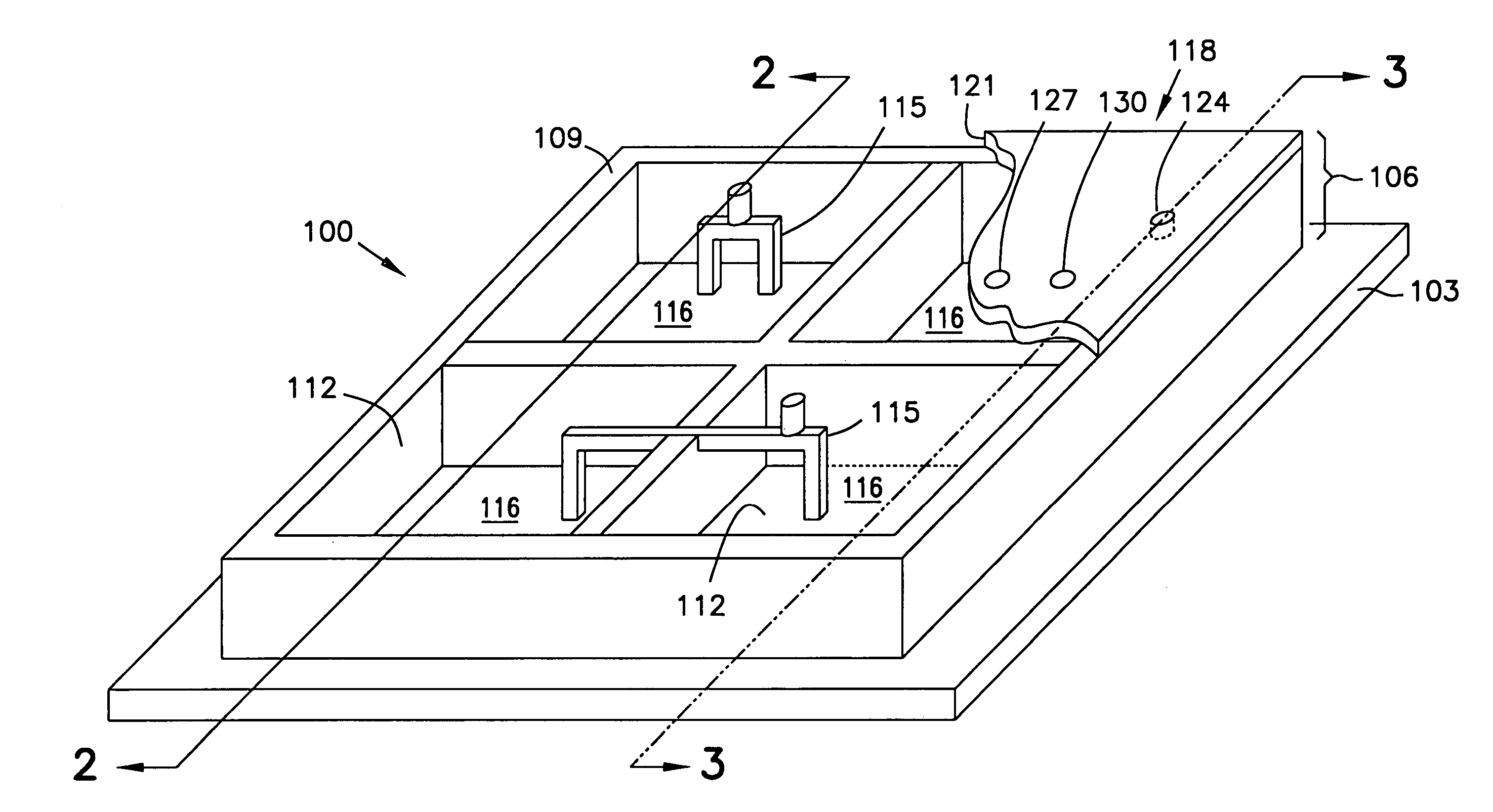
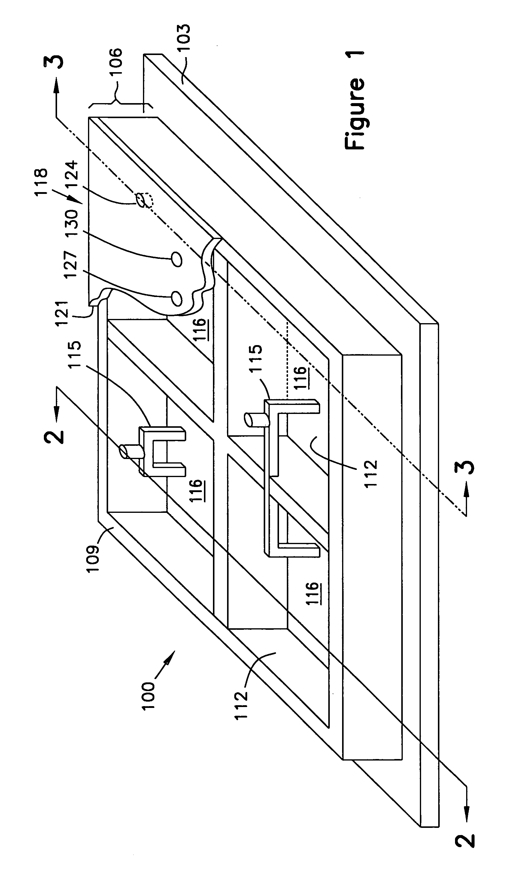
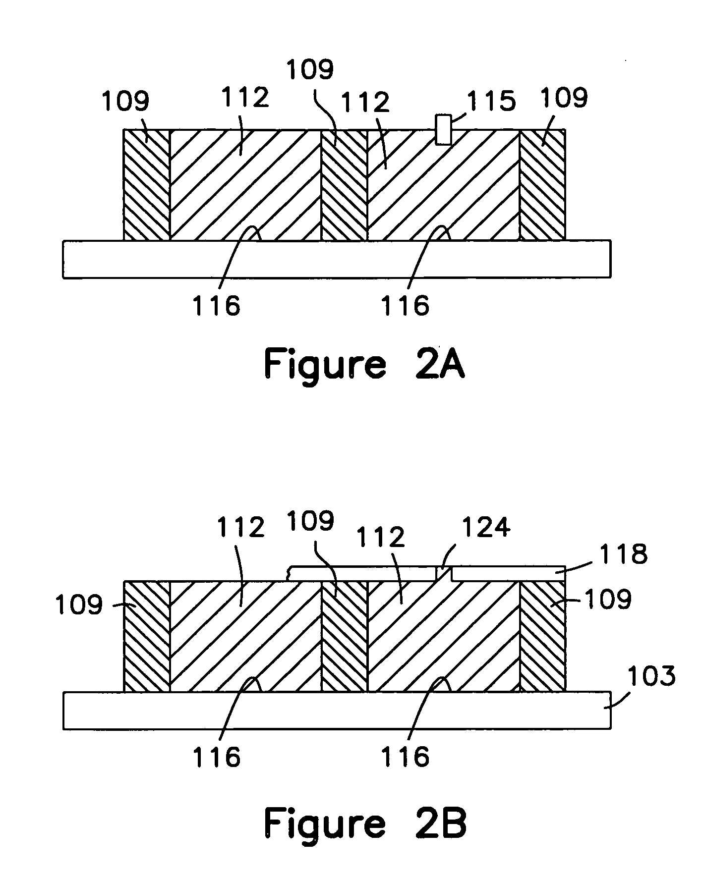
[0019]FIG. 1 is a cutaway perspective view of some embodiments of integrated circuit assembly 100 of the present invention. Integrated circuit assembly 100, in one embodiment, includes electronic chip 103, and material layer 106, comprising ribbed su...


PUM


Abstract

A circuit assembly for fabricating an air bridge structure and a method of fabricating an integrated circuit package capable of supporting a circuit assembly including an air bridge structure. A circuit assembly comprises an electronic chip and a conductive structure embedded in a plurality of materials having a plurality of vaporization temperatures. The plurality of materials is formed on the electronic chip and the conductive structure is coupled to the electronic chip. To fabricate the circuit assembly, a support structure, including interstices, is formed on an electronic chip. The interstices of the support structure are filled with a material having a vaporization temperature that is less than the vaporization temperature of the support structure. Conductive structures are embedded in the support structure and the material, and a connective structure is mounted on the support structure. Finally, the material is removed from the interstices by heating the circuit assembly.

Description

RELATED APPLICATIONS [0001] This application is a Divisional of U.S. application Ser. No. 10 / 931,510 filed Sep. 1, 2004, which is a Divisional of U.S. application Ser. No. 09 / 382,929, filed Aug. 25, 1999, which are incorporated herein by reference.FIELD OF THE INVENTION [0002] This invention relates to the packaging of electronic chips, and more particularly to the packaging of electronic chips having air-bridge structures. BACKGROUND OF THE INVENTION [0003] As the density of devices, such as resistors, capacitors, and transistors, in an integrated circuit is increased, the distance between the signal carrying conductors is decreased, and the capacitive coupling between the conductors is increased. Several problems result from the increased capacitive coupling. First, the increased capacitive coupling reduces the rate at which information can be transferred along each of the signal carrying conductors. Second, the increased capacitive coupling between the signal carrying conductors ...

Claims


Application Information

Patent Timeline
Patent Type & Authority Applications(United States)
IPC IPC(8): H01L21/768H01L23/20H01L23/48H01L23/495H01L23/522H01L23/532H01L23/66H01L29/00
CPCH01L21/7682H01L23/20H01L23/3677H01L23/4821H01L23/5222H01L23/5329Y10S438/977H01L23/66H01L2924/1433H01L2924/0002H01L2924/00
Inventor FARRAR, PAUL A.
Owner MICRON TECH INC
Why Eureka
Try Eureka