Control method and control circuit for laser diode, and optical transmitter using the same

a control method and control circuit technology, applied in the direction of laser details, semiconductor lasers, electrical devices, etc., can solve the problems of deterioration in waveform, increase in jitter of optical transmission signals, so as to prevent deterioration of optical signal characteristics, easy adjustment, and high-density packaging

Inactive Publication Date: 2005-12-29
APRESIA SYST LTD
View PDF10 Cites 22 Cited by
  • Summary
  • Abstract
  • Description
  • Claims
  • Application Information

AI Technical Summary

Benefits of technology

[0039] In the control method for laser diode of the invention, a bias current is adjusted by controlling the bias current of laser diode while feeding back a measurement result of optical output and a modulation current is adjusted based on slope efficiency or its corresponding value. Therefore, the method allows the easy adjustment in manufacturing, the prevention of deterioration in optical signal characteristic and the high-density packaging.
[0040] In the control circuit...

Problems solved by technology

However, as the transmission rate of optical signal is increased, if the extinction ratio is too big, the oscillation of LD cannot follow, causing deterioration in waveform and an increase in jitter of the optical transmission signal.
This causes deterioration in waveform after the long-distance transmission depending on a dispersion characteristic of optical fiber, and the identification sensitivity deteriorates by contrast.
However, the conventional LD control methods (1) to (4) each have problems as follows.
Further, in method (1), since individual difference in temperature characteristic of LD is big, it is difficult to conduct the adjustment in manufacturing.
In method (2), when the tran...

Method used


Image

  • Control method and control circuit for laser diode, and optical transmitter using the same
  • Control method and control circuit for laser diode, and optical transmitter using the same
  • Control method and control circuit for laser diode, and optical transmitter using the same

Examples


first embodiment

(Composition of Optical Transmitter)

[0049]FIG. 3 is a circuit diagram showing an optical transmitter in the first preferred embodiment of the invention.

[0050] The optical transmitter 100 is composed of: LD (laser diode) 1 that emits to an optical waveguide etc. laser light with intensity according to a bias current and a modulation current; a modulation circuit 2 that generates a modulation current to be applied to the LD 1; a current source 3 that applies current to the modulation circuit 2; a current source 4 that applies bias current to the LD 1; a photodiode (PD) 5, light receiving element that is optically coupled to the backward output of LD 1 to monitor the optical output of LD 1; an optical output measurement circuit 6; a temperature measurement circuit 7 that measures a surrounding temperature; a microprocessor 8 as a controller with a program installed therein; a nonvolatile memory 9 that is connected to the microprocessor 8 and stores target values of optical output an...

second embodiment

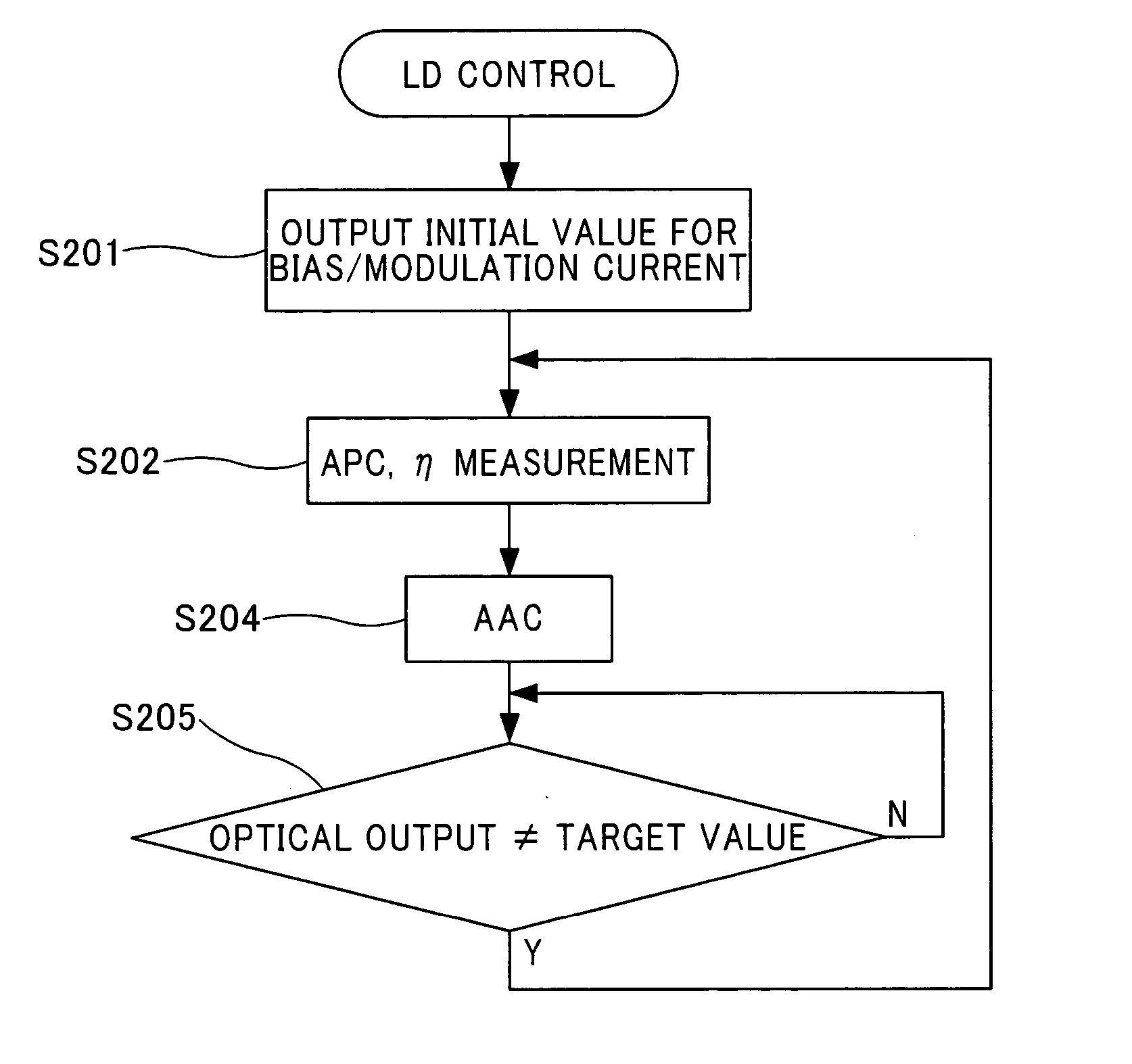
[0058]FIG. 4 is a flowchart showing a control method for laser diode in the second preferred embodiment of the invention as well as showing the operation of the optical transmitter in the first embodiment. The method or operation is conducted by the microprocessor 8. In FIG. 4, S means a step.

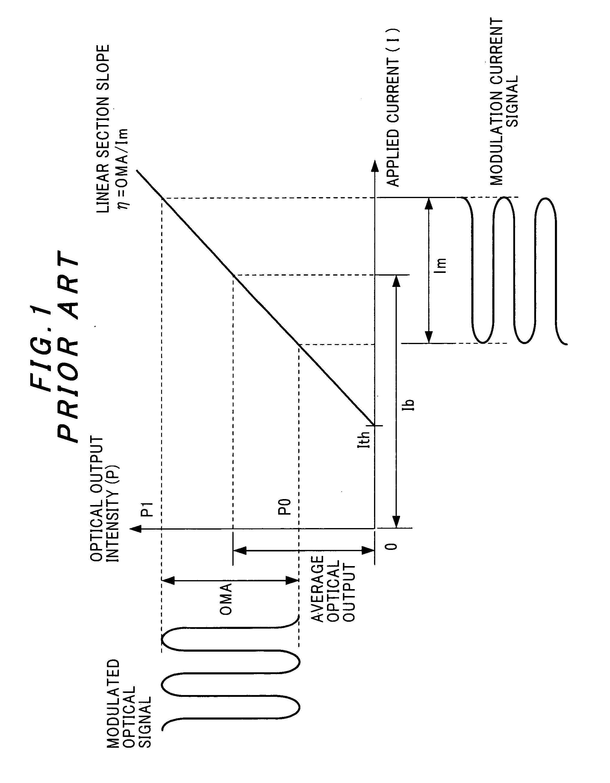
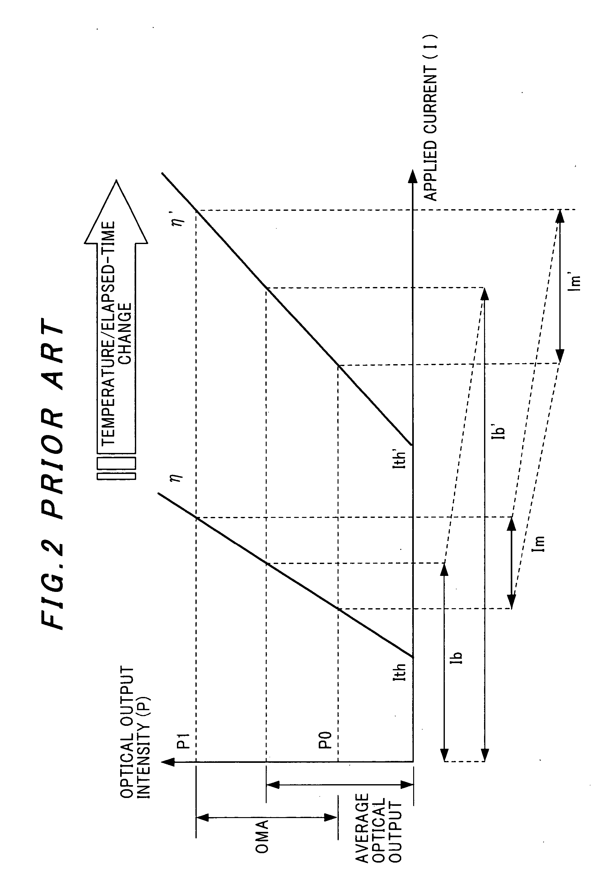
[0059]FIG. 5 is a characteristic diagram showing the relationship between a variation in optical output and bias current and a variation in slope efficiency.

[0060] Referring to FIG. 3 to 5, the control method for laser diode and the operation of microprocessor will be explained below.

[0061] In the second embodiment, the optical output and OMA (optical modulation amplitude) are automatically controlled according to the temperature change and elapsed-time change of oscillation threshold Ith and slope efficiency η.

[0062] First, the microprocessor 8 outputs the initial values of bias current Ib and modulation current Im to control the current sources 3 and 4 (S201). These initial values are mad...

third embodiment

(Method of Controlling the Laser Diode)

[0071]FIG. 6 shows a control method for laser diode in the third preferred embodiment of the invention. In FIG. 6, S means step.

[0072] The third embodiment is different from the second embodiment in the procedures of S201 and S202 as described in the second embodiment. The processing shown in FIG. 6 is also conducted by the microprocessor 8 based on the program stored in the nonvolatile memory 9.

[0073] The microprocessor 8 conducts the procedures in S201, and then it measures a variation of bias current ΔIb, as a corresponding value of η, varied with the change of optical output (S202). Then, it is judged whether or not ΔP (variation of optical output)=ΔPs (preset value) (S301). If the ΔP measured by the optical output measurement circuit 6 coincides with the predetermined ΔPs, the processing of microprocessor 8 is shifted to S204. In S204, a modulation current Im is outputted in proportional to the measured ΔIb. After that, until the optic...


PUM


Abstract

A control method for a laser diode is conducted such that optical output and OMA (optical modulation amplitude) or extinction ratio of the laser diode are controlled while modulating the optical output of the laser diode by applying a bias current and a modulation current to the laser diode. The method has: a first step of measuring the optical output of the laser diode; a second step of measuring a slope efficiency or a corresponding value of the slope efficiency while conducting APC (automatic power control) to adjust the bias current such that the optical output coincides with a predetermined value; and a third step of adjusting the modulation current by AAC (automatic amplitude control) according to the slope efficiency or the corresponding value of the slope efficiency such that the OMA or extinction ratio coincides with a predetermined value.

Description

[0001] The present application is based on Japanese patent application No. 2004-190371, the entire contents of which are incorporated herein by reference. BACKGROUND OF THE INVENTION [0002] 1. Field of the Invention [0003] This invention relates to a control method and a control circuit for a laser diode (LD) and, particularly, to a control method and a control circuit that can cope with a change in optical output intensity of LD due to a temperature change and an elapsed-time change, and further relates to an optical transmitter using the same. [0004] 2. Description of the Related Art [0005] An optical transmitter used for optical communications is equipped with a light source to output light with an intensity according to a bias current and a modulation current, and a modulation circuit to generate the modulation current according to a transmission signal. A transmission signal (herein, a digital signal with a voltage corresponding to logical “1” or “0”) sent from an external devi...

Claims


Application Information

Patent Timeline
IPC IPC(8): H01S3/13H01S5/062
CPCH01S5/06213
Inventor HATTORI, KEITA
Owner APRESIA SYST LTD
Why Eureka
Try Eureka