

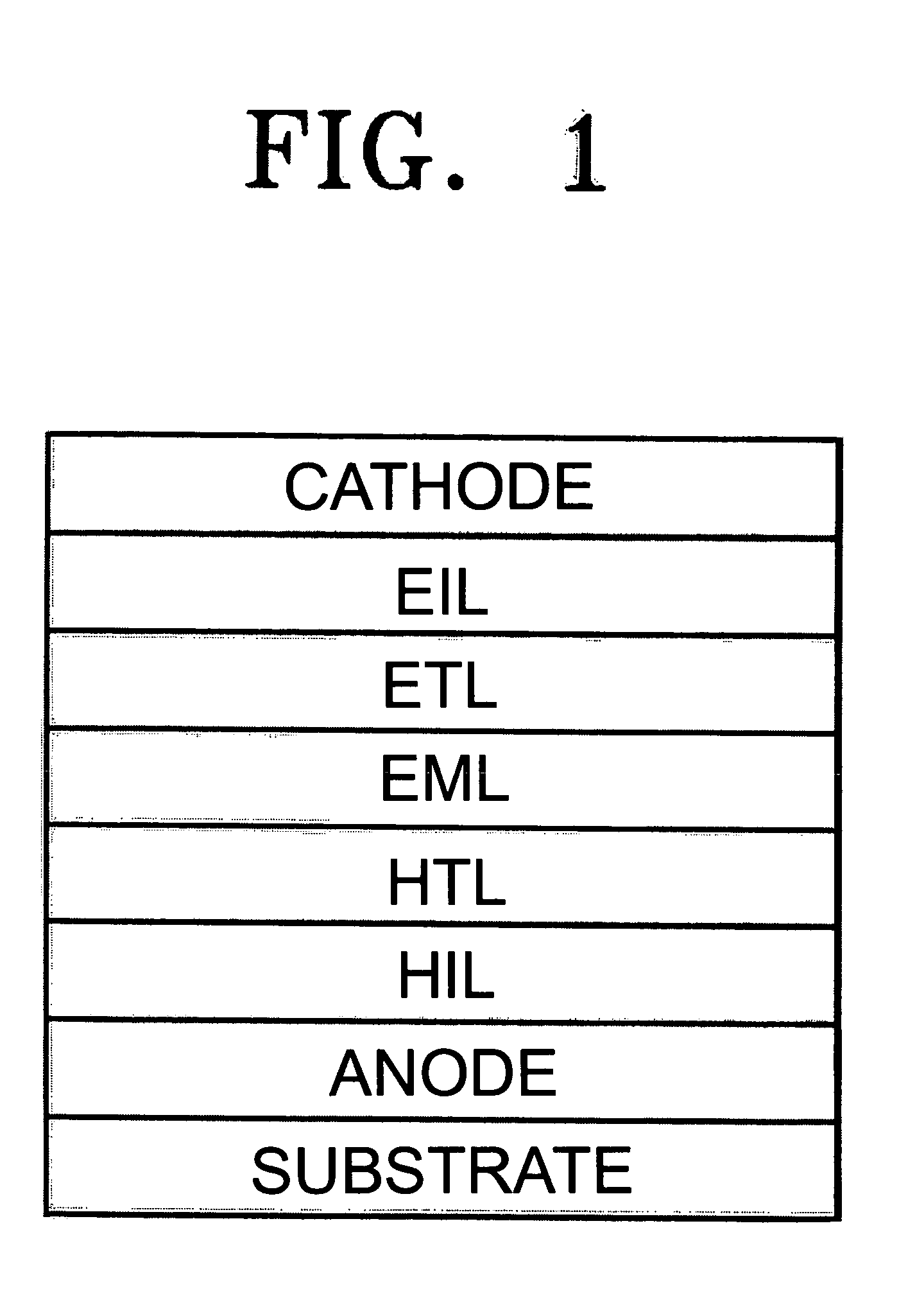
Organic electroluminescent device
a technology of electroluminescent devices and organic materials, applied in the direction of discharge tubes/lamp details, luminescnet screens, natural mineral layered products, etc., can solve the problems of low blue-emission efficiency and short device lifetime, device using carbazole-based phosphorescent materials still have unsatisfactory and achieve enhanced emission efficiency and lifetime characteristics
- Summary
- Abstract
- Description
- Claims
- Application Information
AI Technical Summary
Benefits of technology
Problems solved by technology
Method used
Image

Examples
example 1
[0044] A corning 15 Ω / cm2 (1,200 Å) ITO glass substrate was cut into pieces of 50 mm×50 mm×0.7 mm in size, followed by ultrasonic cleaning in isopropyl alcohol and deionized water (5 minutes for each) and thenUV / ozone cleaning (30 minutes), to be used as an anode.
[0045] A hole transport layer was formed to a thickness of 600 Å on the substrate by vacuum deposition of N,N′-di(1-naphthyl)-N,N′-diphenylbenzidine (NPD).
[0046] A light emission layer was formed to a thickness of about 400 Å on the hole transport layer by co-deposition of a mixture of 50 parts by weight of (4-biphenylyl)-5-(4-t-butylphenyl)-1,3,4-oxdadiazole with an electron transport property and 50 parts by weight of 4,4′-biscarbazolylbiphenyl with a hole transport property as a host and 10 parts by weight of bis(benzothienylpyridine)acetylacetonate iridium as a phosphorescent dopant.
[0047] An electron transport layer was formed to a thickness of about 300 Å on the light emission layer by deposition of Alq3 used as an...
PUM
| Property | Measurement | Unit |
|---|---|---|
| size | aaaaa | aaaaa |
| organic | aaaaa | aaaaa |
| phosphorescent | aaaaa | aaaaa |
Abstract
Description
Claims
Application Information