Transistor, method of fabricating the same, and light emitting display comprising the same

a technology of transistor and light emitting display, which is applied in the direction of identification means, instruments, static indicating devices, etc., can solve the problems of relatively heavy and bulky crt displays

Active Publication Date: 2005-12-29
SAMSUNG DISPLAY CO LTD
View PDF4 Cites 23 Cited by
  • Summary
  • Abstract
  • Description
  • Claims
  • Application Information

AI Technical Summary

Benefits of technology

[0008] Accordingly, it is an aspect of the present invention to provide a transistor which prevents static electricity between metal layers thereof, a method of fabricating the same, and a light emitting display comprising the same.

Problems solved by technology

Recently, various flat panel displays have been developed, and they are substitutes for cathode ray tube (CRT) displays because the CRT displays are relatively heavy and bulky.

Method used


Image

  • Transistor, method of fabricating the same, and light emitting display comprising the same
  • Transistor, method of fabricating the same, and light emitting display comprising the same
  • Transistor, method of fabricating the same, and light emitting display comprising the same

Examples


Embodiment Construction

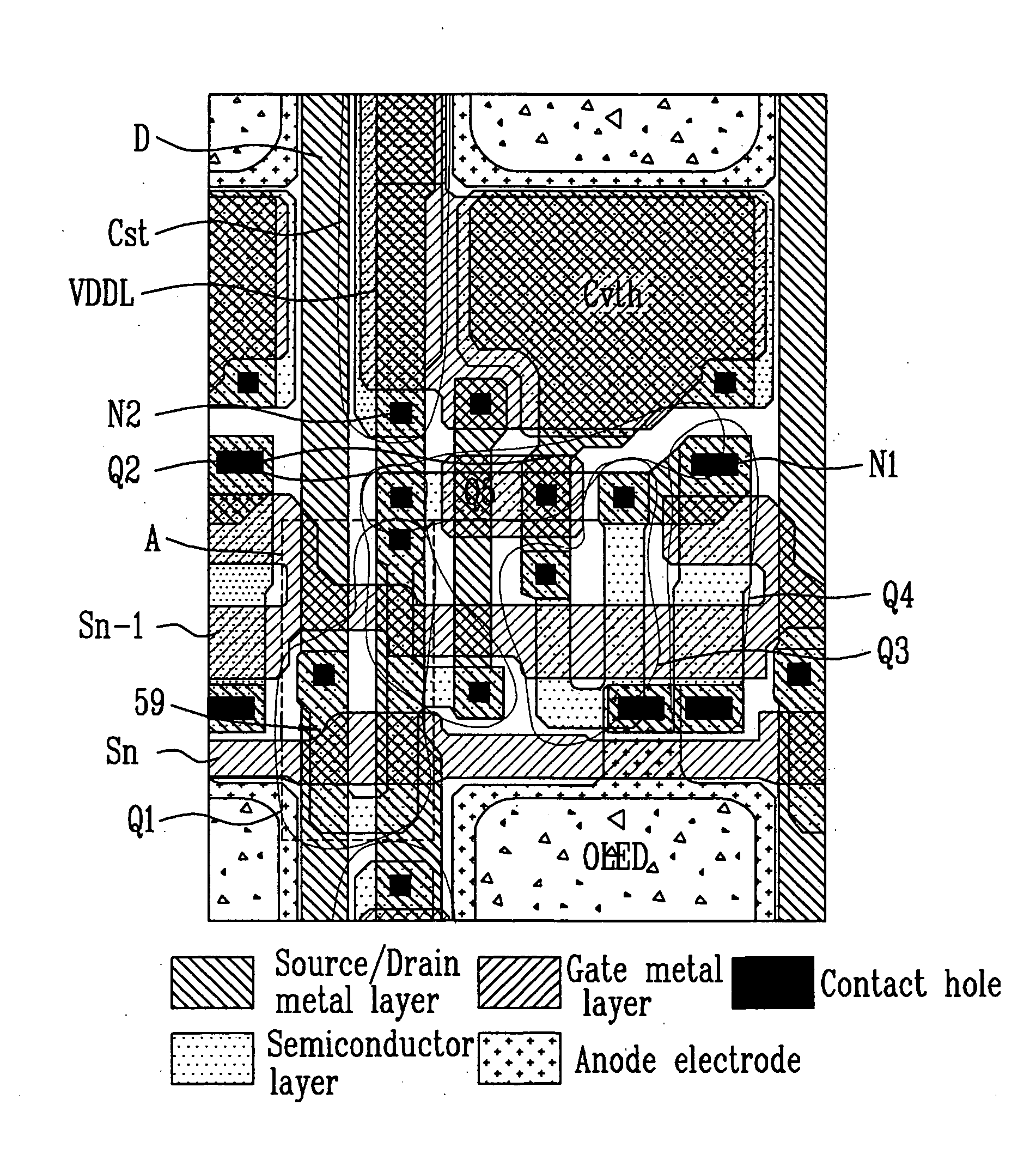
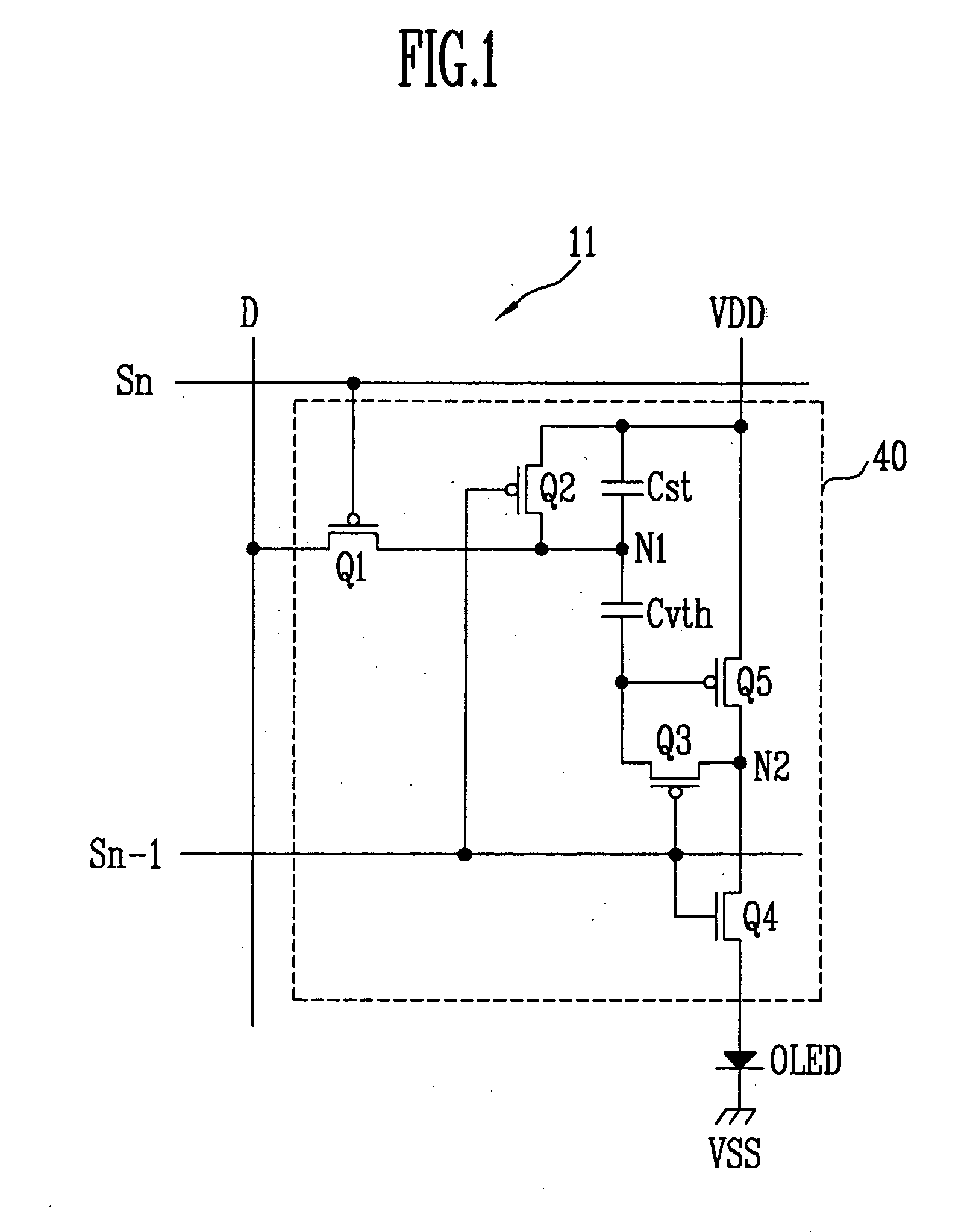
[0030]FIG. 1 is a circuit diagram of a pixel in a light emitting display.

[0031] Referring to FIG. 1, in the light emitting display, a pixel 11 is selected when a scan signal is applied to a scan line S, and the pixel 11 emits light corresponding to a data signal applied to a data line D.

[0032] Each pixel 11 is placed where the data line D and the scan line S cross each other. Pixel 11 comprises an organic light emitting device (OLED) disposed between a first power source VDD and a second power source VSS lower than the first power source VDD, with a pixel circuit 40 being connected to both the data line D and the scan line S and driving the OLED to emit the light.

[0033] The OLED has an anode electrode connected to the pixel circuit 40, and a cathode electrode connected to the second power source VSS. Furthermore, the OLED comprises an emitting layer, an electron transport layer, and a hole transport layer, which are interposed between the anode electrode and the cathode electrode...


PUM


Abstract

A light emitting display comprises: at least one first metal layer; a second metal layer crossing the first metal layer and having a first width; a light emitting device formed adjacent to a region where the first metal layer and the second metal layer cross each other; and a pixel circuit including at least one transistor which causes the light emitting device to emit light. The transistor comprises a semiconductor layer having a second width greater than the first width. With this configuration, in the light emitting display of the present invention, the semiconductor layer of the transistor is formed in a region where the source / drain metal layer and the gate metal layer cross each other, and has a width greater than that of the source / drain metal layer, so that the source / drain metal layer is disposed within the width of the semiconductor layer. Thus, a tip of the gate metal layer, formed in the grain and the pattern edge of the semiconductor layer, is not disposed within the region overlapping the source / drain metal layer so that generation of static electricity between the gate metal layer and the source / drain metal layer is prevented.

Description

CLAIM OF PRIORITY [0001] This application makes reference to, incorporates the same herein, and claims all benefits accruing under 35 U.S.C. §119 from an application entitled TRANSISTOR AND FABRICATION METHOD THEREOF AND LIGHT EMITTING DISPLAY filed with the Korean Intellectual Property Office on 25 Jun. 2004, and there duly assigned Serial No. 2004-48321. BACKGROUND OF THE INVENTION [0002] 1. Technical Field [0003] The present invention relates to a transistor, a method of fabricating the same and, a light emitting display comprising the same and, more particularly, to a transistor preventing static electricity between metal layers thereof, a method of fabricating the same, and a light emitting display comprising the same. [0004] 2. Related Art [0005] Recently, various flat panel displays have been developed, and they are substitutes for cathode ray tube (CRT) displays because the CRT displays are relatively heavy and bulky. The flat panel display can be a liquid crystal display (L...

Claims


Application Information

Patent Timeline
Patent Type & Authority Applications(United States)
IPC IPC(8): H05B33/00G09F9/30G09G3/32H01L21/00H01L21/336H01L21/77H01L27/12H01L27/15H01L27/32H01L29/26H01L29/786H01L31/12H01L51/50
CPCG09G3/3233G09G2300/0852H01L27/124G09G2310/0251H01L27/3244G09G2300/0861H10K59/12H01L27/12H01L27/1214
Inventor LEE, KEUN-SOO
Owner SAMSUNG DISPLAY CO LTD
Why Eureka
Try Eureka