Method for removing electricity and method for manufacturing semiconductor device

a technology of semiconductor devices and electricity removal, which is applied in the testing/measurement of individual semiconductor devices, semiconductor/solid-state devices, instruments, etc., can solve the problems of changing electrical characteristics or damage to circuits, dust can be easily attached to products, and the yield of manufacturing semiconductor devices can be improved, and the static electricity with which a substrate is charged in the manufacturing process of a semiconductor device can be favorably reduced.

Active Publication Date: 2012-09-18
SEMICON ENERGY LAB CO LTD
View PDF129 Cites 21 Cited by
  • Summary
  • Abstract
  • Description
  • Claims
  • Application Information

AI Technical Summary

Benefits of technology

[0010]A significant change in electrical characteristics of thin film transistors and a deviation thereof from the designed range due to static electricity can be suppressed, and the yield in manufacturing semiconductor devices can be improved.
[0011]An object of an embodiment of the present invention is to prevent a substrate from being charged with static electricity in a manufacturing process of a semiconductor device.
[0012]Another object is to favorably reduce static electricity with which a substrate is charged in a manufacturing process of a semiconductor device.

Problems solved by technology

In a manufacturing plant where semiconductor devices are manufactured, in a manufacturing process of, for example, semiconductor elements, ICs, liquid crystal panels, magnetic heads, or the like, static electricity may adversely affect electronic circuits and cause a change in electrical characteristics or damage to circuits.
In addition, there is also a problem in that static electricity causes dust to be easily attached to products.

Method used


Image

  • Method for removing electricity and method for manufacturing semiconductor device
  • Method for removing electricity and method for manufacturing semiconductor device
  • Method for removing electricity and method for manufacturing semiconductor device

Examples


embodiment 1

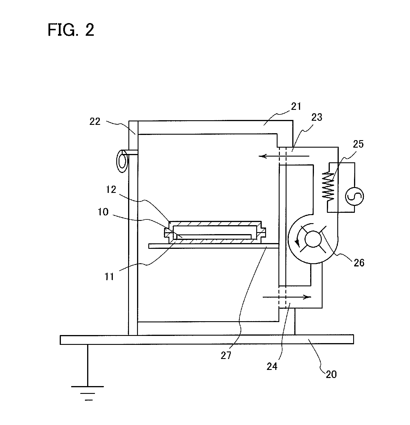
[0055]In this embodiment, heat treatment with a substrate surrounded using a tray body and a tray cover will be described below.

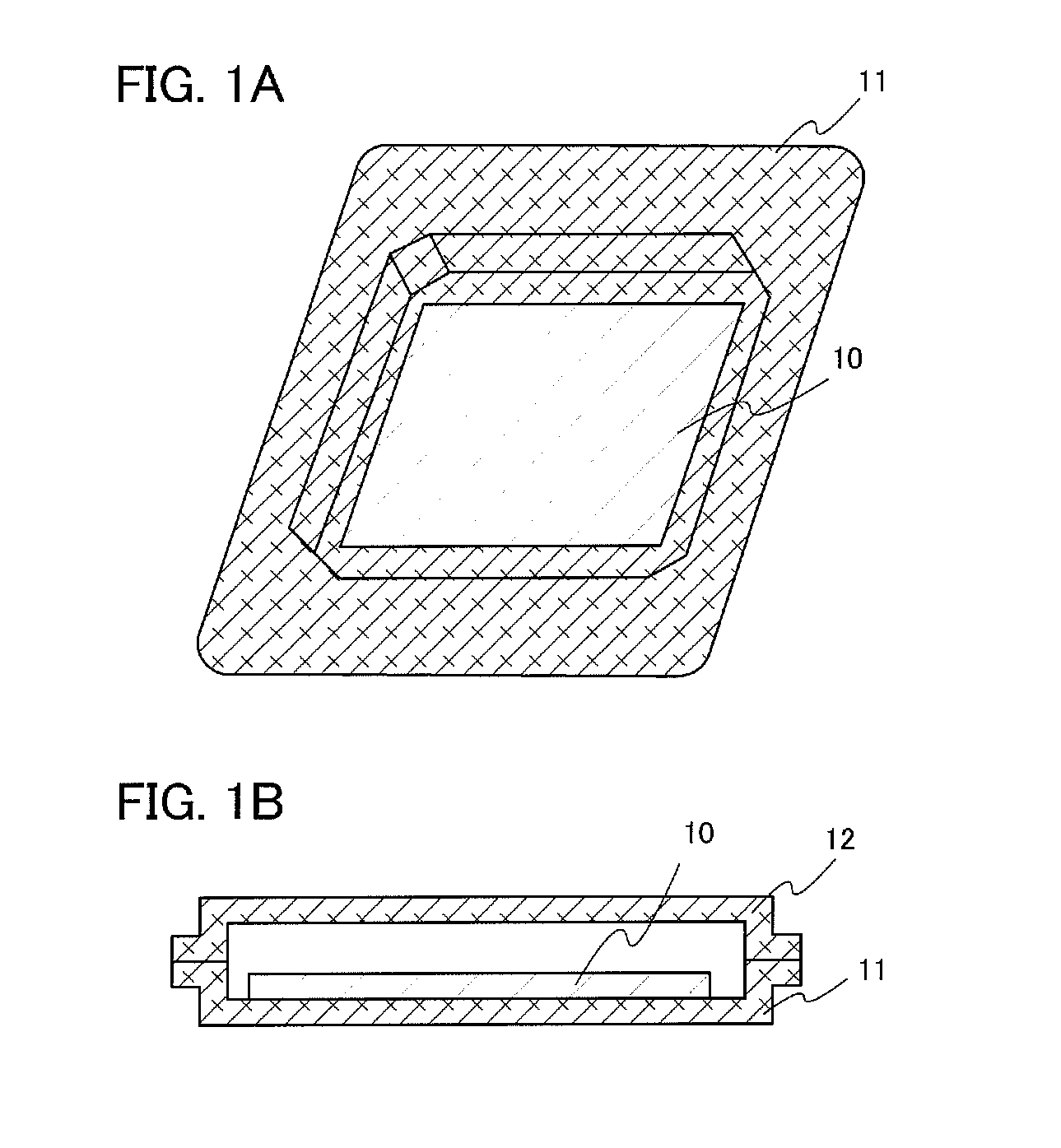
[0056]FIG. 1A is an external view illustrating a state in which a substrate 10 is placed in a depressed portion of a tray body 11.

[0057]The substrate 10, for which a glass substrate or the like is used, is provided with a circuit including a thin film transistor on one side. Note that the shape of the substrate 10 is not particularly limited to a quadrangular shape and may be a circular shape or the like, for example.

[0058]The tray body 11 is formed using a conductive material such as aluminum, copper, titanium, molybdenum, tungsten, or niobium. In this embodiment, aluminum is used.

[0059]Then, a tray cover 12 is placed so as to overlap the tray body 11 such that the substrate 10 is surrounded as shown in a cross-sectional view of FIG. 1B. Then, the peripheral portion of the tray body 11 and the tray cover 12 is hermetically sealed with kapton tape or the li...

embodiment 2

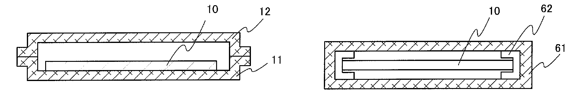
[0120]In Embodiment 1, an example in which a tray with a cover is used as a storage container for a substrate is described; in this embodiment, a container having a quadrangular prism shape is used.

[0121]FIG. 6A is a schematic diagram illustrating a state shortly before a substrate 10 is put in a container 61 having a quadrangular prism shape. In this embodiment, the container 61 is illustrated as storing a substrate in a state where one substrate surface is directed vertical. Note that FIG. 6B is a top view of the container 61 in a state after the substrate 10 is stored therein, and a substrate holding member 62 is provided in contact with the substrate. For the container 61, a conductive material such as aluminum, copper, titanium, molybdenum, tungsten, or niobium is used. The substrate holding member 62 is also preferably formed using a conductive material.

[0122]Note that FIGS. 6A and 6B illustrate the container 61 which is configured to store only one substrate, whereas the cont...

embodiment 3

[0126]In Embodiments 1 and 2, examples of using containers are described; in this embodiment, metal foil is wrapped around a substrate, which is placed on the shelf of the heating apparatus in FIG. 2 and heated while being electrically connected to a ground potential.

[0127]FIG. 7A is an external view in which one substrate 10 is wrapped in metal foil 71. FIG. 7B is a cross-sectional view thereof.

[0128]As a material of the metal foil 71, aluminum, copper, titanium, molybdenum, tungsten, niobium, or the like is used. In this embodiment, aluminum foil is used.

[0129]A sheet of aluminum foil may be used to wrap the substrate 10, or a plurality of sheets, two or more sheets, of aluminum foil may be used to wrap the substrate 10. In addition, it is preferable that a substrate is put in a hollow space surrounded by aluminum foil, which is hermetically sealed with kapton tape or the like so as not to expose the substrate to ambient air.

[0130]A substrate wrapped in aluminum foil is placed on ...


PUM


Abstract

An object is to suppress a significant change in electrical characteristics of thin film transistors and a deviation thereof from the designed range due to static electricity, and to improve the yield in manufacturing semiconductor devices. In order to prevent a substrate from being charged with static electricity by heat treatment or to favorably reduce static electricity with which a substrate is charged in a manufacturing process of a semiconductor device, heat treatment is performed with a substrate provided with a thin film transistor stored in a conductive container. In addition, a heating apparatus for performing the heat treatment is electrically connected to a ground potential, and the container and the substrate are also electrically connected to the ground potential.

Description

TECHNICAL FIELD[0001]The present invention relates to a method for removing static electricity in a manufacturing plant where semiconductor devices are manufactured. The present invention also relates to a method for manufacturing a semiconductor device which has a circuit including a thin film transistor (hereinafter referred to as a TFT). For example, the present invention relates to electronic devices which are mounted with electro-optical devices typified by liquid crystal display panels, or light emitting display devices including an organic light emitting element, as a component.[0002]In this specification, a semiconductor device generally means a device which can function by utilizing semiconductor characteristics, and an electro-optical device, a semiconductor circuit, and an electronic device are all semiconductor devices.BACKGROUND ART[0003]In a manufacturing plant where semiconductor devices are manufactured, in a manufacturing process of, for example, semiconductor eleme...

Claims


Application Information

Patent Timeline
Patent Type & Authority Patents(United States)
IPC IPC(8): H01L21/00H01L21/469H01L21/31H01L51/40H01L21/66
CPCH01L27/1225H01L29/66969H01L29/7869H01L29/78603
Inventor YOSHITOMI, SHUHEITSUBUKU, MASASHIYAMAZAKI, SHUNPEI
Owner SEMICON ENERGY LAB CO LTD
Why Eureka
Try Eureka