Semiconductor manufacturing apparatus and semiconductor manufacturing method

a manufacturing apparatus and semiconductor technology, applied in mechanical equipment, manufacturing tools, grinding drives, etc., can solve problems such as the possibility of causing a problem, the circuit of the front surface, and the defect of the semiconductor wafer

Active Publication Date: 2008-06-19
RENESAS ELECTRONICS CORP
View PDF2 Cites 21 Cited by
  • Summary
  • Abstract
  • Description
  • Claims
  • Application Information

AI Technical Summary

Benefits of technology

[0022]According to the present invention, in supporting of a semiconductor by a vacuum chuck, a product can be prevented from being influenced by static electricity.

Problems solved by technology

The wafer front surface 4 is damaged due to the static electricity, as a result, a circuit thereof may be a defect.
In more detail, under a status described below, there is a possibility of causing a problem.
In a planarization process for an oxidized film on interconnections, this static electricity may destroy an insulation layer on the interconnections.
Furthermore, in a process for polishing a surplus of a metal layer embedded in grooves and holes, a metal existing in a dimple may melt because of the electric charge.

Method used


Image

  • Semiconductor manufacturing apparatus and semiconductor manufacturing method
  • Semiconductor manufacturing apparatus and semiconductor manufacturing method
  • Semiconductor manufacturing apparatus and semiconductor manufacturing method

Examples


Embodiment Construction

[0031]The invention will be now described herein with reference to illustrative embodiments. Those skilled in the art will recognize that many alternative embodiments can be accomplished using the teachings of the present invention and that the invention is not limited to the embodiments illustrated for explanatory purposes.

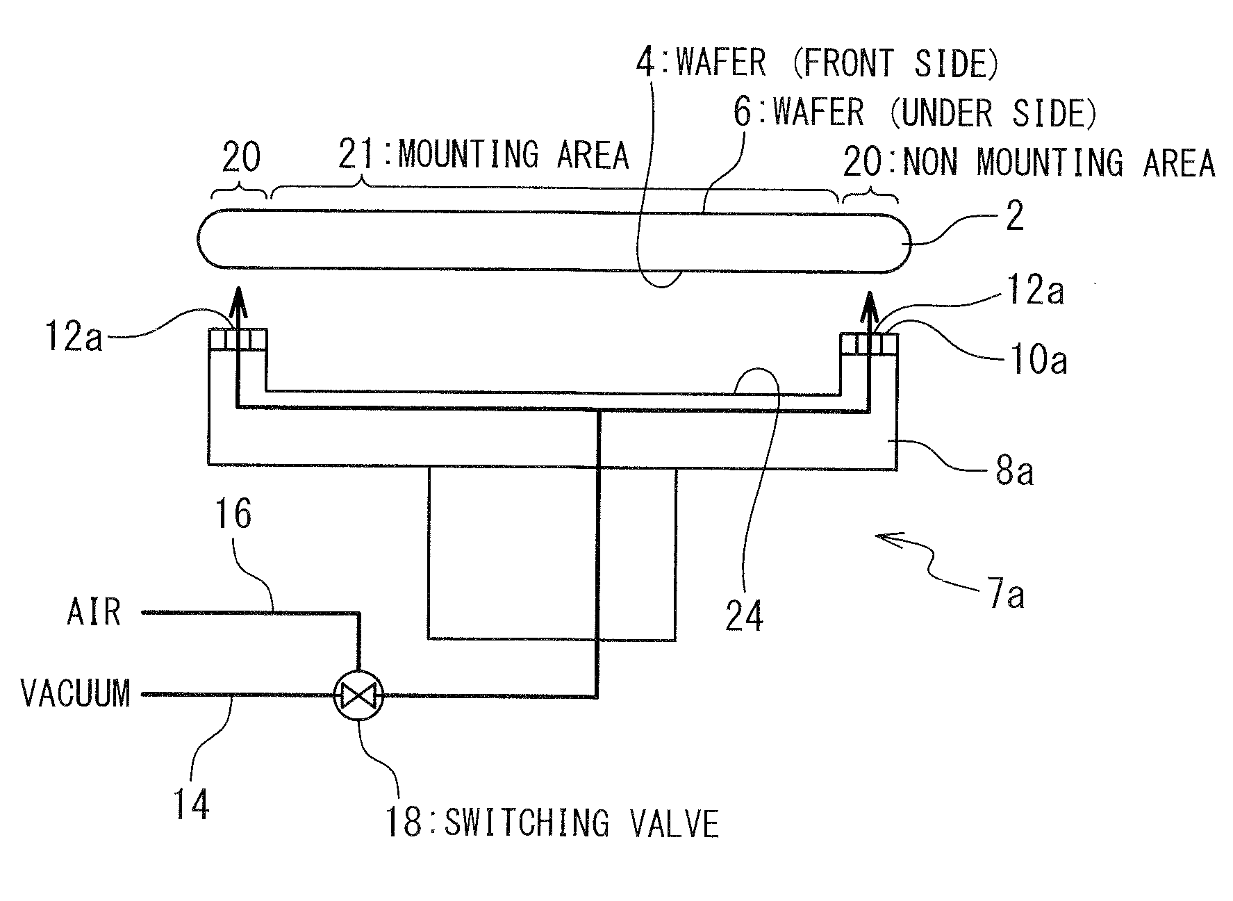
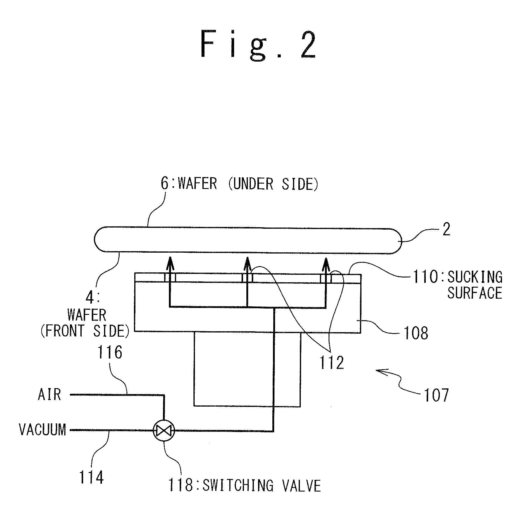
[0032]Referring now to FIG. 4, a side view of a transit mechanism 7 in a first embodiment of the present invention is shown. The transit mechanism 7 includes a supporting unit (which is also called as a supporting member) 8, a vacuuming system 14, a gas supply system 16, and a switching valve 18. The shape of the supporting unit 8 is symmetry of rotation against a central axis parallel with a vertical direction. An upper surface of the supporting unit 8 is a flat sucking surface 10 for supporting the semiconductor wafer 2 horizontally.

[0033]Wafer sucking openings 12 are formed in the supporting unit 8 and open on the sucking surface 10. The wafer sucking openings...


PUM


Abstract

A semiconductor manufacturing apparatus includes a supporting unit for supporting a semiconductor wafer received from a CMP apparatus and a vacuuming system for holding the wafer on the supporting unit. The vacuuming is applied only in a peripheral area of the wafer. In the peripheral area of the wafer, any circuit such as interconnections and devices are not manufactured. When the wafer is released by supplying gas to the vacuumed space, even if static electricity occurs, the electronic circuit to be manufactured on the wafer does not harmed, because the static electricity occurs only in the peripheral area where any circuit does not exist.

Description

[0001]This application is related to Japanese Patent Application No. 2006-336172. The disclosure of that application is incorporated herein by reference.BACKGROUND OF THE INVENTION[0002]1. Field of the Invention[0003]The present invention relates to a technique for holding a semiconductor wafer by a vacuum chuck.[0004]2. Description of Related Art[0005]In a manufacturing process of a semiconductor device, a vacuum chuck is used for holding a semiconductor wafer.[0006]FIG. 1 shows a part of a semiconductor manufacturing process using a vacuum chuck. A semiconductor wafer is mounted on a wafer cassette (step S1). A transit mechanism takes out the semiconductor wafer from the wafer cassette, and passes it to a CMP (Chemical Mechanical Polishing) apparatus (step S2). The semiconductor wafer is attached to a polishing head of the CMP apparatus. The semiconductor wafer is polished with a CMP process (step S3). The transit mechanism receives the semiconductor wafer treated with the CMP pro...

Claims


Application Information

Patent Timeline
Patent Type & Authority Applications(United States)
IPC IPC(8): B24B5/02B23B31/30
CPCB23B31/307Y10T279/11H01L21/6838
Inventor MORITA, TOMOTAKE
Owner RENESAS ELECTRONICS CORP
Why Eureka
Try Eureka