Light emitting element and method of making same

a technology of light-emitting elements and light-emitting elements, which is applied in the direction of basic electric elements, semiconductor devices, electrical equipment, etc., can solve the problems of large current that cannot be applied thereto, difficult to enhance brightness or improve light-emitting, and non-uniform light patterns, etc., to achieve increased emission area, increase brightness thereof, and prevent uneven light-emitting patterns

Inactive Publication Date: 2006-01-05
TOYODA GOSEI CO LTD
View PDF8 Cites 60 Cited by
  • Summary
  • Abstract
  • Description
  • Claims
  • Application Information

AI Technical Summary

Benefits of technology

[0038] In the invention, since the p-type and n-type electrodes can be varied in arbitrary form, the light emitting element can have an increased emission area relative to the element's surface area and prevent unevenness in light distribution so as to increase brightness thereof.
[0039] Further, the light emitting element can have an excellent mounting performance, a high reliability in electrical connection, and a heat radiation performance even in a large size type.
[0040] In addition, the method of making the light emitting element can be conducted by using the conventional apparatus without requiring any advance technique.

Problems solved by technology

Therefore, a large current cannot be applied thereto since the current density of the light-emitting layer becomes too high.
Further, since about ¼ of the element's surface area becomes nonradiative portion due to the n-electrode area, a non-uniform light pattern is generated.
Therefore, it is difficult to enhance the brightness or to improve the light distribution.
Thus, since each chip needs to be processed by using a microscopic and advanced technique, it is difficult to produce the LED element in mass production.
Further, in the LED element, although the electrical connection performance is enhanced, the heat radiation performance is insufficient for heat generated during the operation.

Method used


Image

  • Light emitting element and method of making same
  • Light emitting element and method of making same
  • Light emitting element and method of making same

Examples


first embodiment

(Composition of LED Element 1)

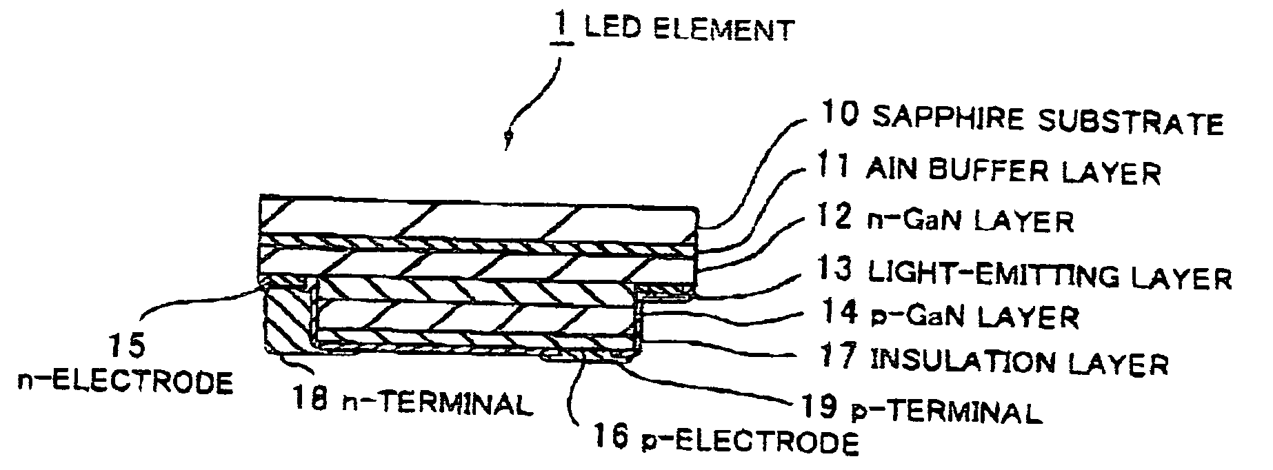
[0090]FIGS. 1A to 1D show an LED element in the first preferred embodiment according to the invention.

[0091] The LED element 1 is composed of: a sapphire substrate 10; an AlN buffer layer 11 formed on the sapphire substrate 10; an n-GaN layer 12 formed on the AlN buffer layer 11; a light-emitting layer 13 formed on the n-GaN layer 12; a p-GaN layer 14 formed on the light-emitting layer 13, the n-GaN layer 12 to the p-GaN layer 14 being of group III nitride-based compound semiconductor; an n-electrode 15 as a second electrode formed on part of the n-GaN layer 12 exposed by partially etching the p-GaN layer 14 to the n-GaN layer 12; a p-electrode 16 as a first electrode formed on the p-GaN layer 14 to supply current to the light-emitting layer 13; an insulation layer 17 of a SiO2-based material formed to cover the electrode formation side; an n-terminal 18 electrically connected through an opening 17n provided in the insulation layer 17 to the n-electr...

second embodiment

(Composition of LED Element 1)

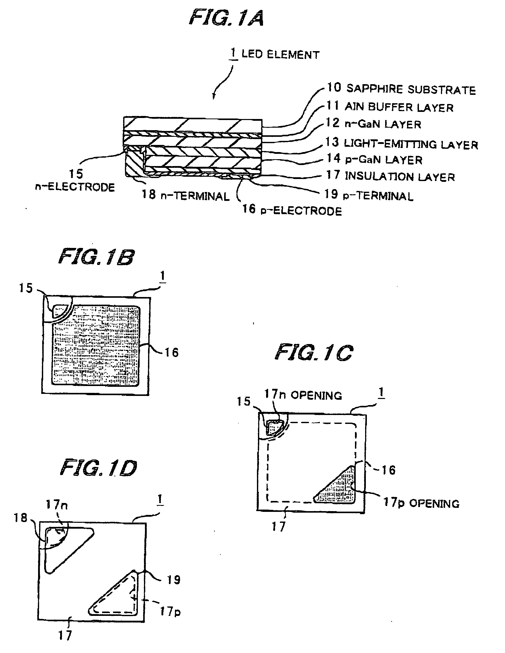
[0113]FIGS. 2A to 2D show an LED element in the second preferred embodiment according to the invention.

[0114] Herein, like components are indicated by the same numerals as used in the first embodiment.

[0115] The flip-chip type LED element 1 is different from the first embodiment in that, as shown in FIG. 2A, the p-GaN layer 14 is disposed like an island at the center of the LED element 1, the p-electrode 16 is formed thereon, and the n-electrode 15 is disposed circularly around the p-electrode 16.

[0116] The n-electrode 15 is about 10 μm in line width of narrowest portion and about 350 μm in line width of widest portion. The p-electrode 16 is, as shown in FIG. 2B, shaped like a square with rounded corners, and a predetermined distance separated through an insulation portion 100 from the n-electrode 15 which circularly surrounds the p-electrode 16. The predetermined distance is preferably such a minimum one that can prevent the light leakage from the...

modification 1

(Modification 1 of Electrode Form)

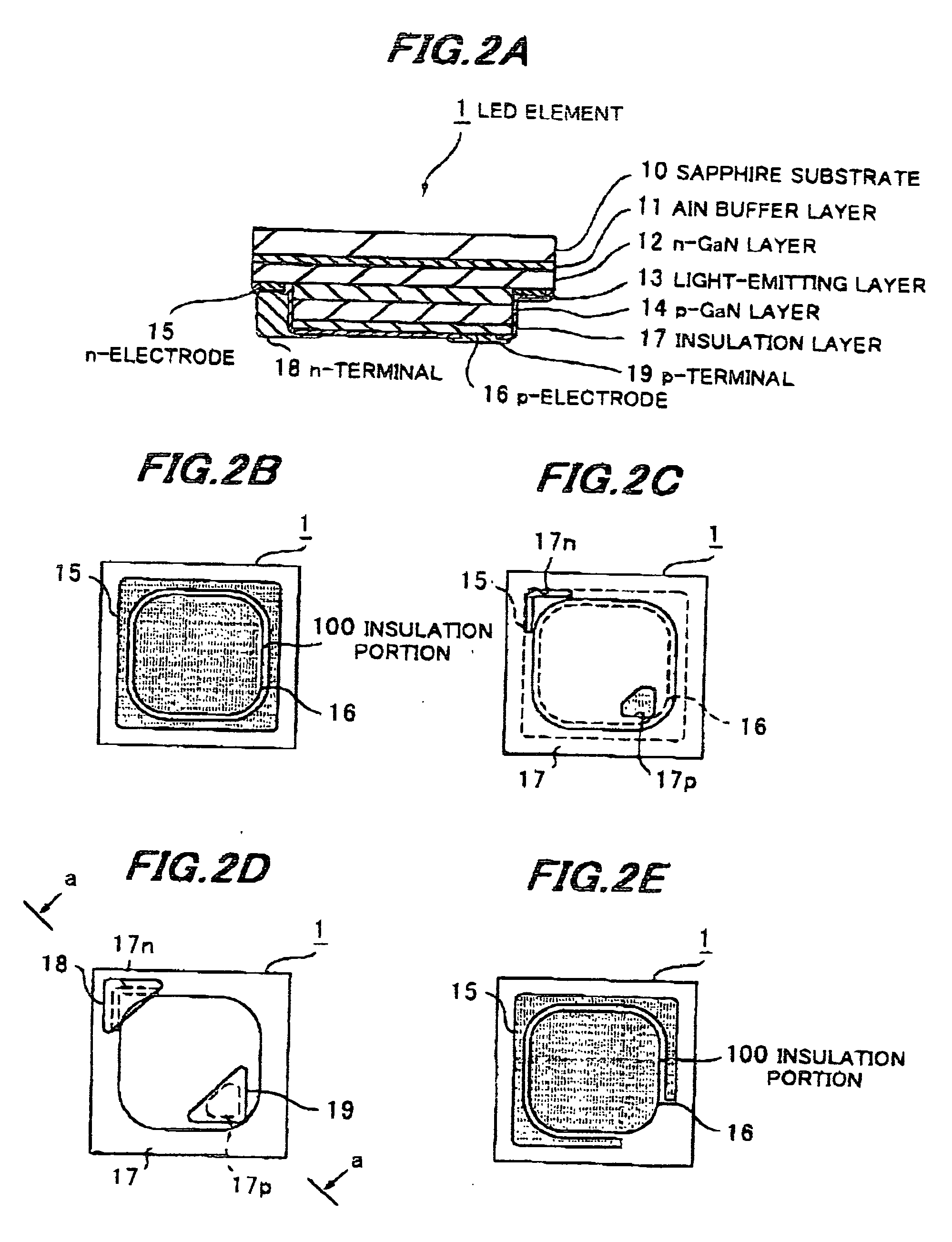
[0125] As shown in FIG. 3A, the n-electrode 15 may have a separation portion 150 that diagonally separates the p-electrode 16.

[0126] In modification 1, since the formation region of the p-electrode 16 is separated into two parts, current can be uniformly and rapidly spread and thereby good emission characteristics can be obtained under the p-electrode 16


PUM


Abstract

A light emitting element has: a semiconductor layer having a light-emitting layer; a first electrode; a second electrode; an insulation layer that is formed on a mounting face side of the semiconductor layer; and a first terminal and a second terminal that are formed on a surface of the insulation layer corresponding to the first electrode and the second electrode, respectively. The first electrode and the second electrode are formed on the mounting face side of the semiconductor layer. The insulation layer has a first opening and a second opening, and the first electrode and the second electrode are electrically connected through the first hole and the second hole, respectively, to the first terminal and the second terminal.

Description

[0001] The present application is based on Japanese patent application Nos. 2004-184028 and 2004-252499, the entire contents of which are incorporated herein by reference. BACKGROUND OF THE INVENTION [0002] 1. Field of the Invention [0003] This invention relates to a light emitting element and, particularly, to a light emitting element that has an increased emission area relative to the element's surface area and prevents unevenness in light distribution so as to increase brightness thereof. Also, this invention relates to a light emitting element that has an excellent mounting performance, a high reliability in electrical connection, and a heat radiation performance as well as having an increased emission area relative to the element's surface area. Further, this invention relates to a method of making the light emitting element thus featured while using the conventional apparatus without requiring any advance technique. [0004] Herein, a light emitting element includes a light emit...

Claims


Application Information

Patent Timeline
Patent Type & Authority Applications(United States)
IPC IPC(8): H01L29/205H01L21/00
CPCH01L33/20H01L33/38H01L2933/0016H01L2924/0002H01L2924/00
Inventor SUEHIRO, YOSHINOBUWADA, SATOSHI
Owner TOYODA GOSEI CO LTD
Why Eureka
Try Eureka