Deposition box for silicon-based thin film solar cell

a solar cell and silicon-based technology, applied in the field of solar cell technology, can solve the problems of low plasma concentration, long deposition period, low deposition rate,

Inactive Publication Date: 2012-06-07
SHEN ZHEN TRONY SCI & TECH DEV CO LTD
View PDF4 Cites 9 Cited by
  • Summary
  • Abstract
  • Description
  • Claims
  • Application Information

AI Technical Summary

Benefits of technology

[0019]The beneficial effects of the present deposition box invention, different from the slot-type cathode plate with side feed modes, include that deposition which achieves the higher uniformity, greater discharge area and the stable discharge performance can be obtained in the deposition box, the connection capacitance is smaller, the actual discharge power is greater, and the radio frequency interference between electrode plate arrays is smaller. Also different from cathode plate center-point-type feed mode of the single chamber deposition system, the connection capacitance is smaller, the standing wave and the skin effect is smaller, and the integrated array type multi-chamber deposition can be obtained to greatly improve production efficiency. Therefore, through optimizing VHF power feed-in form and electrode plate structure, the solution of RF / VHF discharge uniformity can be obtained, and it is the premise of high efficient preparation technology for crystallized silicon thin film. The invention is applicable for any power and any legitimate VHF frequencies in the range of 27.12 MHz 200 MHz for large area uniform discharge. This structure can be applied to multiple-glasses deposition systems for greatly improving the productivity and reducing the cost of solar cells. The invention breaks through the conventional electrode design technical limitations, effectively eliminates the VHF inducing effects such as a standing wave and the skin effect, and improves uniform discharge to industrial application level.

Problems solved by technology

However, in a microcrystalline environment, plasma generated by 13.56 MHz RF may have low plasma concentration, low deposition rate, long deposition period to reach targeted film thickness, and significant background pollution.
Thus, the prepared thin film often has high impurity and poor photoelectric properties, which seriously affects the quality and performance of the products.
However, the following problems may still remain: 1) The electrodes in the VHF-PECVD chamber have complex design structures; 2) One reason for the continuous improvement is that the constant assembly / disassembly and cleaning of the reaction chamber and electrodes can cause abnormal deformation of the electrodes; 3) The multi-point feed-in structures disclosed in the existing patents may have a small contact surface, which requires symmetrical paths of individual feed-in points and there is no contact between the bonding conductors at the feed-in points and the cathode plate.
These structural designs have relatively harsh actual requirements, have too many determination factors for uniform discharge, and cannot meet the actual production needs such as disassembly and cleaning.
But due to the standing wave effect and the skin effect, current single-point feed-in structures cannot meet the requirement for increasing the high feed-in frequency.

Method used


Image

  • Deposition box for silicon-based thin film solar cell
  • Deposition box for silicon-based thin film solar cell
  • Deposition box for silicon-based thin film solar cell

Examples


embodiment 1

[0031]Electrode plates are vertically placed. Cathode plates have circular feed-in ports, and feed-in components have flat waists and semi-circular feed-in interfaces.

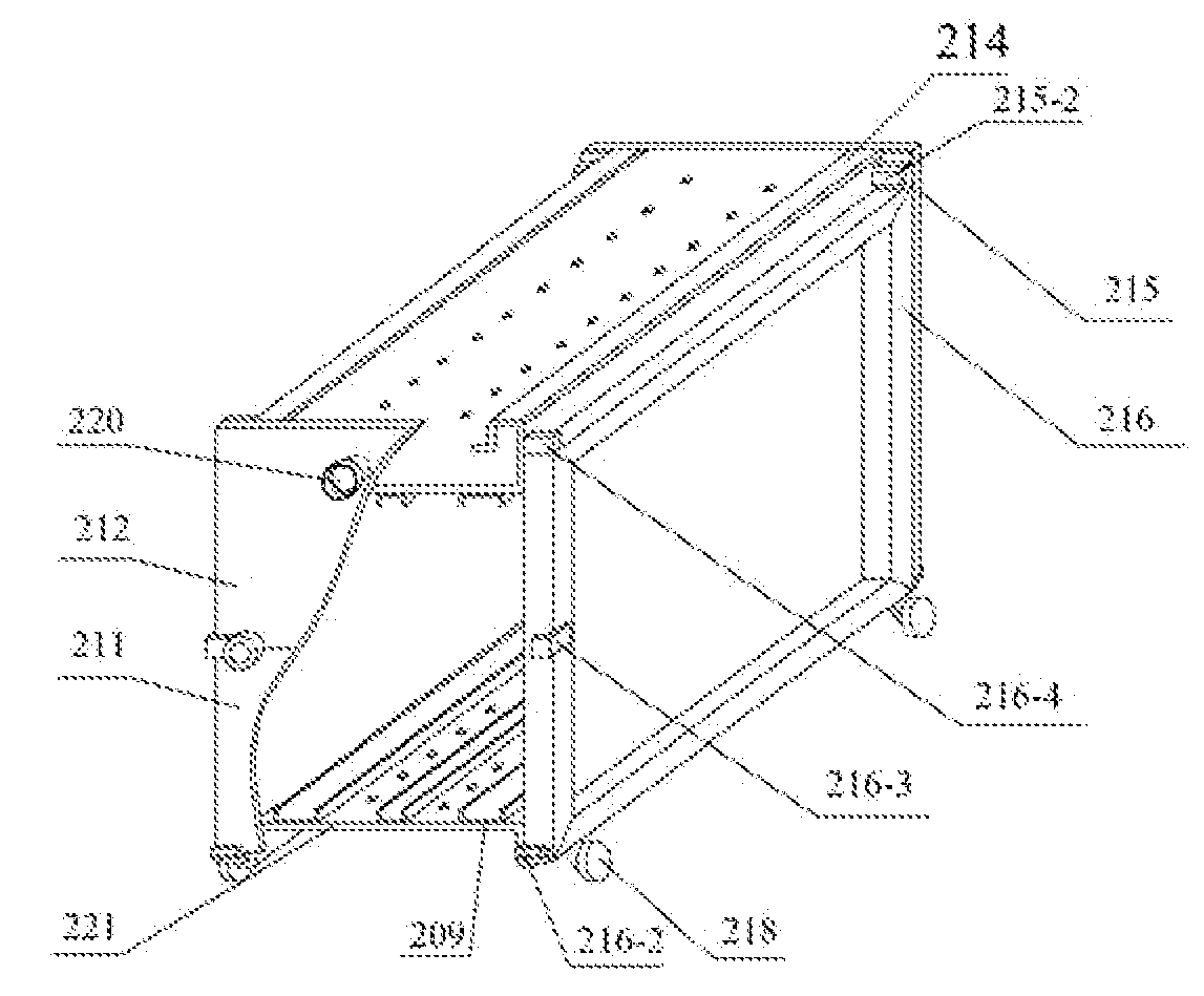
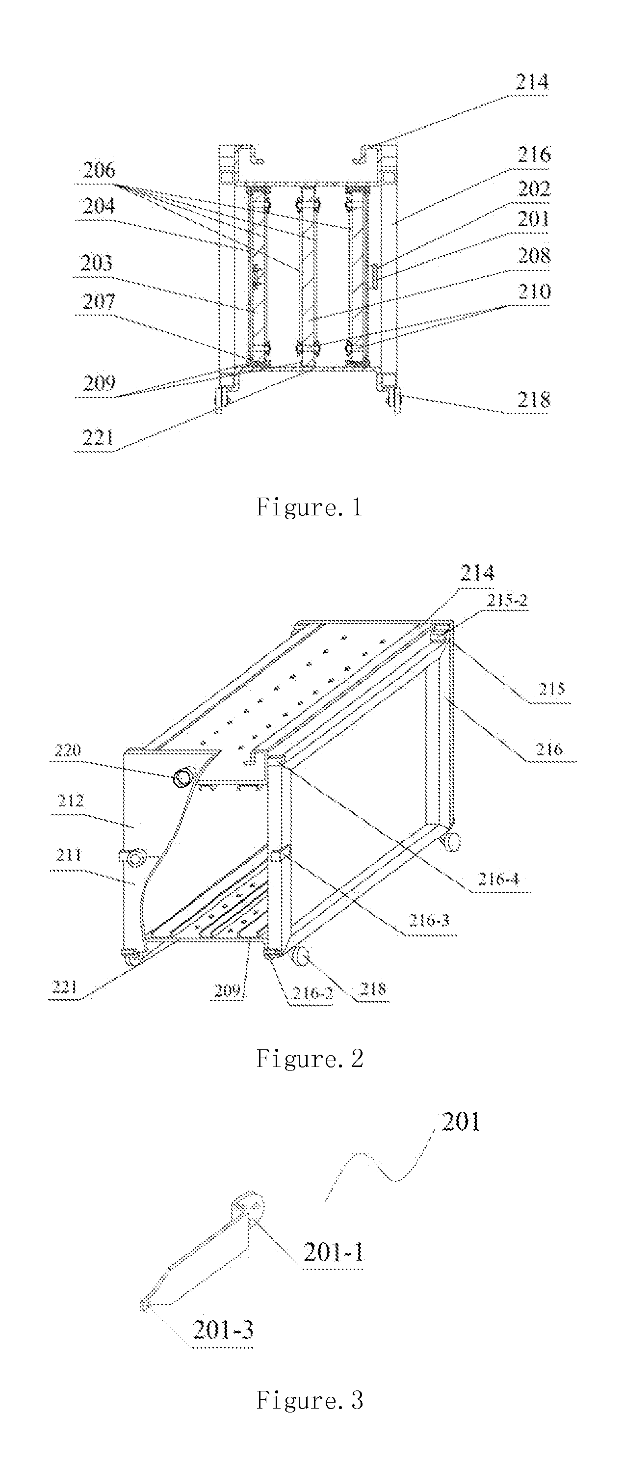
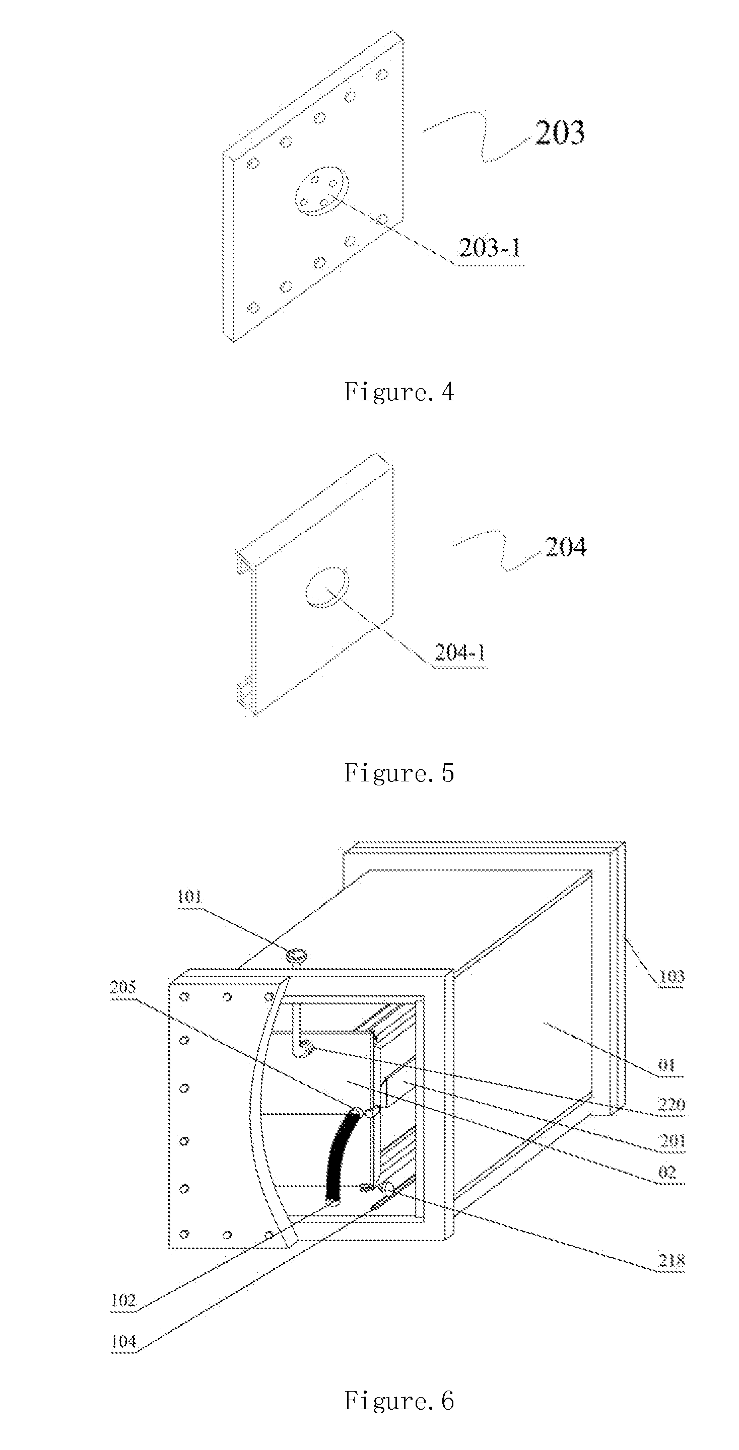
[0032]The principle of this embodiment is illustrated with FIGS. 1-6. In deposition box 02, two cathode plates 203 surround one anode plate 208. PECVD deposition system consists of vapor deposition chamber, gas system, electrical power system, vacuum system, heating system, control system, and so on. Gas system mainly provides different gases and gas lines for vapor deposition. Electrical power system mainly provides high-frequency or very-high-frequency electrical power source to discharge plasma for film deposition. Vacuum system mainly provides vacuum pumping machines and vacuum pipelines. Heating system mainly supplies heat for vapor deposition chamber. Control system mainly controls the parameters of deposition process. Vapor deposition chamber is the apparatus for realizing thin film deposition with gases on subs...

embodiment 2

[0035]Electrode plates are vertically placed. Cathode plates have circular feed-in ports. Feed-in components have flat waists and semi-circular feed-in interface. Cathode plates are insulated from shields and through holes are set in the shields of cathode plates.

[0036]Deposition box in FIG. 7 is the same as that in Embodiment 1, in which 8 glass substrates 206 can be processed at the same time. Two cathode plates 203 surround one anode plate 208, and four pairs of electrodes can be formed by two anode plates 208 and four cathode plates 203. In such a configuration, eight substrates can be coated with thin films at the same time. Detailed processes are illustrated as follows:

[0037]a) Place 8 glass substrates (1640 mm×707 mm×3 mm) with 600-nm transparent conducting thin films in the substrate position in deposition box 02. Film side of the substrate faces outside, while glass side of the substrate faces toward electrode plate.

[0038]b) Open the active door 103 of the vacuum chamber, a...

embodiment 3

[0045]Electrode plates are vertically placed. Cathode plates have circular feed-in ports. Feed-in components have flat waists and semi-circular feed-in interface. Cathode plates are insulated from shields and through holes are set in the shields of cathode plates.

[0046]Deposition box in FIG. 8 is the same as that in Embodiment 1, in which 24 glass substrates 206 can be processed at the same time. Two cathode plates 203 surround one anode plate 208, and twelve pairs of electrodes can be formed by six anode plates 208 and twelve cathode plates 203. In such a configuration, twenty four substrates can be coated with thin films at the same time. Detailed processes are illustrated as follows:

[0047]a) Place 24 glass substrates 206 (1640 mm×707 mm×3 mm) with 600-nm transparent conducting films in the substrate position in deposition box 02. Film side of the substrate faces outside, while glass side of the substrate faces toward electrode plate.

[0048]b) Open the active door 103 of the vacuum...


PUM

PropertyMeasurementUnit
frequencyaaaaaaaaaa
frequencyaaaaaaaaaa
excitation frequencyaaaaaaaaaa

Abstract

A movable deposition box (02) for silicon-based thin film solar cell comprises an electrode array composed of at least a group of cathode plates (203) and a piece of anode plate (208) which are set in movable chamber, wherein a feeding socket (203-1) is positioned on a circular or semicircular concave surface in the center area on the backside of the cathode plates (203), a circular or semicircular end face (201-1) of a feeding component (201) which has a flat middle part contacts the signal feeding socket (203-1) and feeds in RF / VHF power signal, the anode plate (208) is grounded, and a shield cover (204) of the cathode plate has through-hole (204-1) and is insulated from the cathode plate (203).

Description

FIELD OF THE INVENTION[0001]The present invention generally relates to solar cell technologies and, more particularly, to a deposition box driven by VHF (27.12 MHz-100 MHz) for silicon-based thin film solar cells.BACKGROUND[0002]Currently, silicon thin film solar cells often use plasma enhanced chemical vapor deposition (PECVD) to deposit single-junction or multi junction photovoltaic PIN film layers. This type of radio-frequency (RF) capacitively-coupled parallel plate reactor is commonly used in the thin film solar cell industry. Deposition process, such as plasma-enhanced chemical vapor deposition, is conducted in the reaction chamber through electrode plate components with electrode plate array. RF capacitively-coupled parallel-plate electrode reaction chamber is widely used in various kinds of large area thin film deposition of amorphous silicon, amorphous silicon germanium, silicon carbide, silicon nitride, and silicon oxide materials, etc. Industry-wide, the electrode with a ...

Claims


Application Information

Patent Timeline
Patent Type & Authority Applications(United States)
IPC IPC(8): C23C16/509H01L31/18H01L31/042
CPCC23C16/24C23C16/509C23C16/545Y02E10/50H01J37/32091H01J37/32577H01J37/32715H01L31/1816H01L31/042H01L31/18
Inventor LI, YI
Owner SHEN ZHEN TRONY SCI & TECH DEV CO LTD
Why Eureka
Try Eureka