Surface feed-in electrodes for deposition of thin film solar cell and signal feed-in method thereof

a solar cell and surface feed-in electrode technology, applied in the field of solar cell technology, can solve the problems of low plasma concentration, long deposition period, low deposition rate,

Inactive Publication Date: 2013-05-14
SHEN ZHEN TRONY SCI & TECH DEV CO LTD
View PDF3 Cites 0 Cited by
  • Summary
  • Abstract
  • Description
  • Claims
  • Application Information

AI Technical Summary

Benefits of technology

[0022]The beneficial effects of the present invention, different from the slot-type cathode plate with side feed modes, include that the present invention can achieve the higher uniformity, greater discharge area and the stable discharge performance. Further, the connection capacitance is smaller, the actual discharge power is greater, and the radio frequency interference between electrode plate arrays is smaller. Also different from cathode plate center-point-type feed mode of the single chamber deposition system, the connection capacitance is smaller, the standing wave and the skin effect is smaller, and the integrated array type multi-chamber deposition can be obtained to greatly improve production efficiency. Therefore, through optimizing VHF power feed-in form and electrode plate structure, the solution of RF / VHF discharge uniformity can be obtained, and it is the premise of high efficient preparation technology for crystallized silicon thin film. The invention is applicable for any power and any legitimate VHF frequencies in the range of 27.12 MHz˜200 MHz for large area uniform discharge. This structure can be applied to multiple-glasses deposition systems for greatly improving the productivity and reducing the cost of solar cells. The invention breaks through the conventional electrode design technical limitations, effectively eliminates the VHF inducing effects such as a standing wave and the skin effect, and improves uniform discharge to industrial application level.

Problems solved by technology

However, in a microcrystalline environment, plasma generated by 13.56 MHz RF may have low plasma concentration, low deposition rate, long deposition period to reach targeted film thickness, and significant background pollution.
Thus, the prepared thin film often has high impurity and poor optical properties, which seriously affects the quality and performance of the products.
However, the following problems may still remain: 1) The electrodes in the VHF-PECVD chamber have complex design structures; 2) One reason for the continuous improvement is that the constant assembly / disassembly and cleaning of the reaction chamber and electrodes can cause abnormal deformation of the electrodes; 3) The multi-point feed-in structures disclosed in the existing patents may have a small contact surface, which requires symmetrical paths of individual feed-in points and there is no contact between the bonding conductors at the feed-in points and the cathode plate.
These structural designs have relatively harsh actual requirements, have too many determination factors for uniform discharge, and cannot meet the actual production needs such as disassembly and cleaning.
But due to the standing wave effect and the skin effect, current single-point feed-in structures cannot meet the requirement for increasing the high feed-in frequency.

Method used


Image

  • Surface feed-in electrodes for deposition of thin film solar cell and signal feed-in method thereof
  • Surface feed-in electrodes for deposition of thin film solar cell and signal feed-in method thereof
  • Surface feed-in electrodes for deposition of thin film solar cell and signal feed-in method thereof

Examples


first embodiment

The First Embodiment

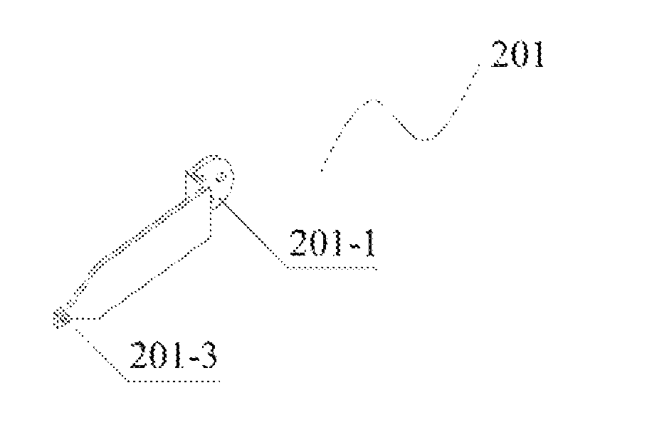
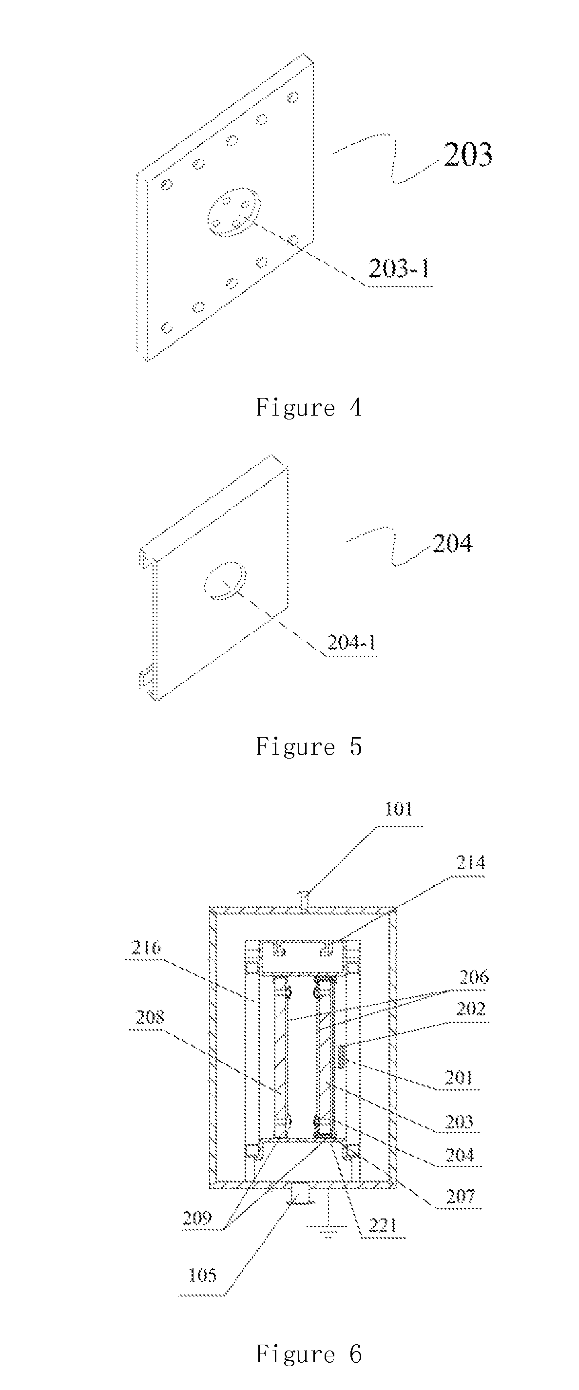
[0035]The electrode plates are arranged vertically, and the feed-in port of cathode is of a circular shape and is located in a hollowed circular area at the center of the backside of the cathode electrode plate. The signal feed-in component includes a flat waist and one end with a semicircular-shaped signal feed-in surface. A through-hole is configured on the cathode shielding cover.

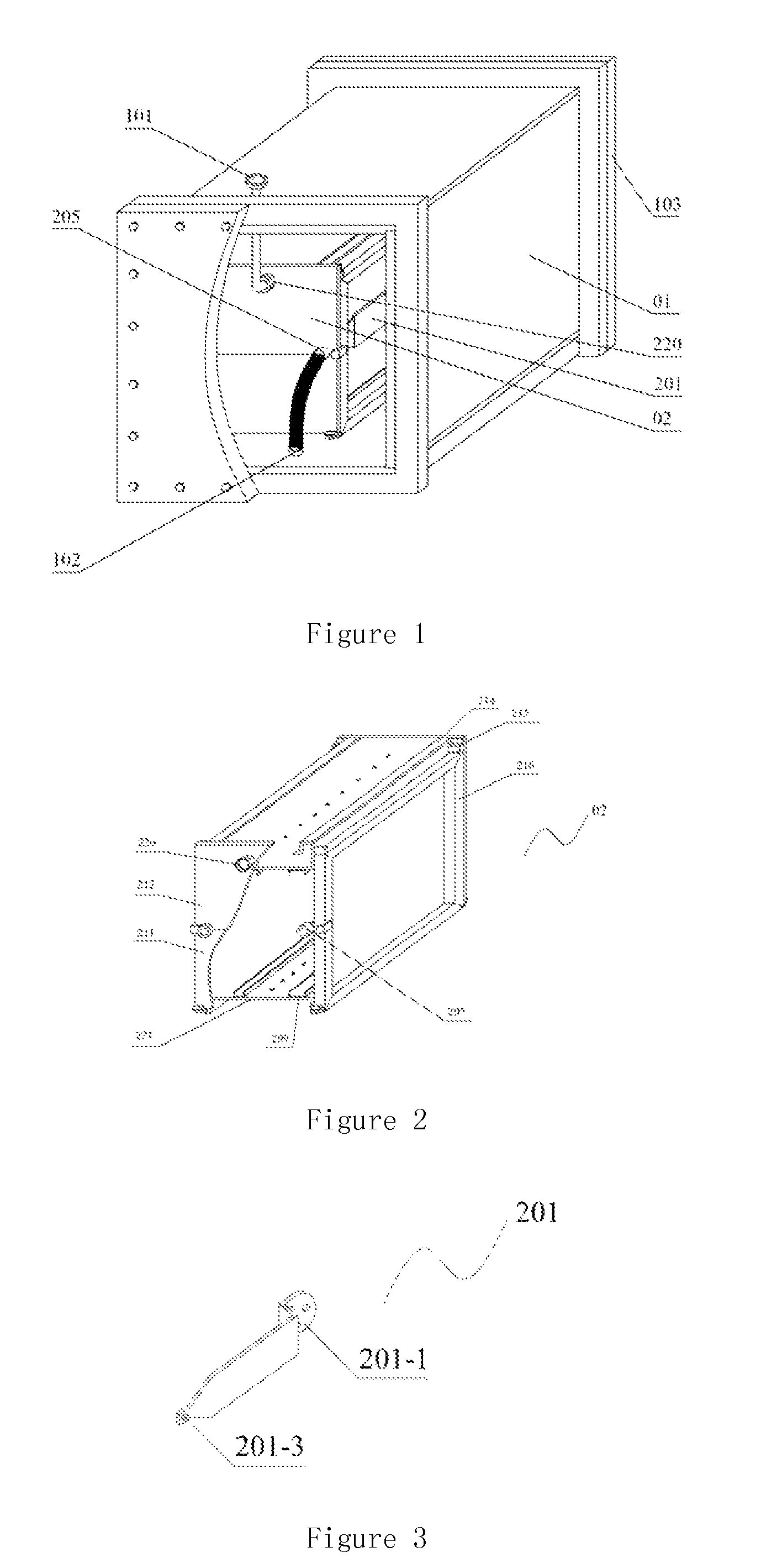
[0036]The principles of this embodiment are illustrated together with accompanying FIGS. 1-6. The vapor deposition system mainly includes a vapor deposition chamber, a gas system, an electrical power system, a vacuum system, a heating system, a control system, and so on. The gas system mainly provides different gases and gas lines for vapor deposition. The electrical power system mainly provides high-frequency or very-high-frequency electrical power source to discharge plasma for film deposition. The vacuum system mainly provides vacuum pumping machines and vacuum pipelines. The heati...

second embodiment

The Second Embodiment

[0043]The feed-in port of the cathode plate is of a circular shape and is located on a circular surface of a hollowed circular area at the center of the backside of the cathode electrode plate. The signal feed-in component includes a flat waist and one end with a semicircular-shaped signal feed-in surface. A through-hole is configured on the cathode shielding cover.

[0044]As shown in FIG. 6, a vertically-arranged reaction chamber is used. An anode plate 208 and a cathode plate 203 form a set of electrodes, and a total of 2 substrates 206 can be deposited with thin film simultaneously. More specifically:

[0045]a) Placing 2 glass substrates 206 (1640 mm×707 mm×3 mm) each coated with a transparent conductive film of approximately 600 nm thickness in the corresponding 2 substrate locations on the reaction chamber 02, with the film side facing outside and the glass side facing the electrode plates.

[0046]b) When reaching a vacuum state of approximately 5.0×10⁻⁴ Pa insid...

third embodiment

The Third Embodiment

[0051]The feed-in port of the cathode plate is of a circular shape and is located on a circular surface of a hollowed circular area at the center of the backside of the cathode electrode plate. The signal feed-in component includes a flat waist and one end with a semicircular-shaped signal feed-in surface. A through-hole is configured on the cathode shielding cover.

[0052]As shown FIG. 7, a horizontal reaction chamber is used. Eight (8) anode plates 208 and eight (8) cathode plates 203 form 8 sets of electrodes, and a total 16 substrates 206 can be deposited with thin film simultaneously. The detailed procedure is described as follows:

[0053]a) Placing 16 glass substrates 206 (1640 mm×707 mm×3 mm) each coated with a transparent conductive film of approximately 600 nm thickness in the corresponding 16 substrate locations on the reaction chamber 02, with the film side facing outside and the glass side facing the electrode.

[0054]b) When reaching a vacuum state of appr...


PUM

PropertyMeasurementUnit
frequencyaaaaaaaaaa
frequencyaaaaaaaaaa
excitation frequencyaaaaaaaaaa

Abstract

The present invention discloses a surface feed-in electrode structure for thin film solar cell deposition, relating to solar cell technologies. The surface feed-in electrode structure uses a signal feed-in component with a flat waist and a semicircular feed-in end to connect the signal feed-in port by surface contact. The signal feed-in port is located in a hallowed circular area of a center of the backside of a cathode plate, and feeds in an RF / VHF power supply signal. An anode plate is grounded. The cathode plate is insulated with a shielding cover, and a through-hole is configured on the shielding cover. The effects include that, by using the surface feed-in at the center of the electrode plate, the feeding line loss of single-point or multi-point feed-in configurations can be overcome. Uniform large area and stable discharge driven by the RF / VHF power supply signal can be achieved, and the standing wave and the skin effect can be effectively removed. The production efficiency can be improved and the cost can be reduced.

Description

FIELD OF THE INVENTION[0001]The present invention generally relates to solar cell technologies and, more particularly, to electrodes used in a very high frequency (VHF) driven silicon-based thin film solar cell deposition chamber.BACKGROUND[0002]Currently, silicon-based thin film solar cells often use plasma enhanced chemical vapor deposition (PECVD) to construct single-junction or multi junction photovoltaic PIN film layers. This type of radio-frequency (RF) capacitively-coupled parallel plate reactor is commonly used for making large-area thin film deposition of various materials, such as amorphous silicon, amorphous silicon-germanium, silicon carbide, silicon nitride and silicon oxide, etc. In the thin film solar cell industry, the electrode with a supporting frame is usually called a clamping unit, a holder, or a fixture, and the plasma chemical vapor deposition apparatus with installed holder(s) inside the chamber is often called the “deposition box,” i.e., the reactor chamber....

Claims


Application Information

Patent Timeline
Patent Type & Authority Patents(United States)
IPC IPC(8): H01J1/00H05H1/24
CPCC23C16/505H01L31/1804H01L31/1824H01J37/32577H01J37/32091C23C16/24Y02E10/545Y02E10/547Y02P70/50
Inventor HU, SHENGMINGLI, YIHE, ZHUBINGLI, ZHIJIANZHOU, JIANHUAWANG, CHUNZHU
Owner SHEN ZHEN TRONY SCI & TECH DEV CO LTD
Why Eureka
Try Eureka