Discharge electrode array for thin-film solar cell deposition
a solar cell and discharge electrode technology, applied in the field of solar cell technology, can solve the problems of low plasma concentration, long deposition period, low deposition rate, etc., and achieve the effects of stable discharge performance, increased discharge area, and stable discharge performan
- Summary
- Abstract
- Description
- Claims
- Application Information
AI Technical Summary
Benefits of technology
Problems solved by technology
Method used
Image
Examples
embodiment 1
[0031
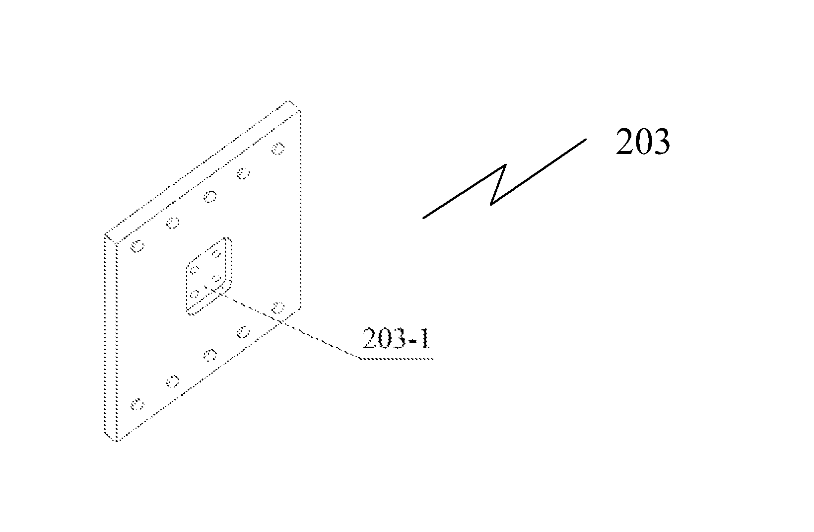
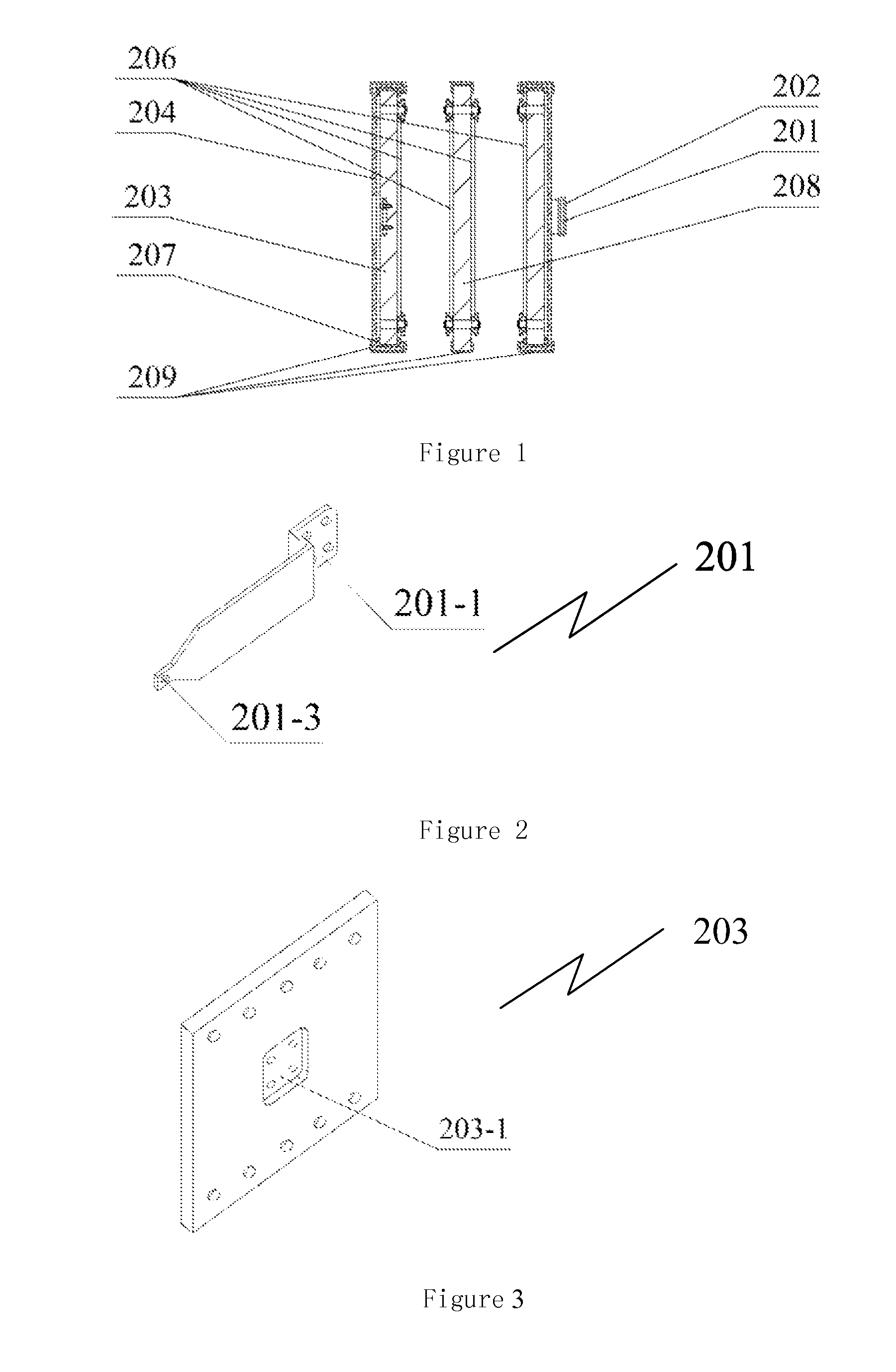
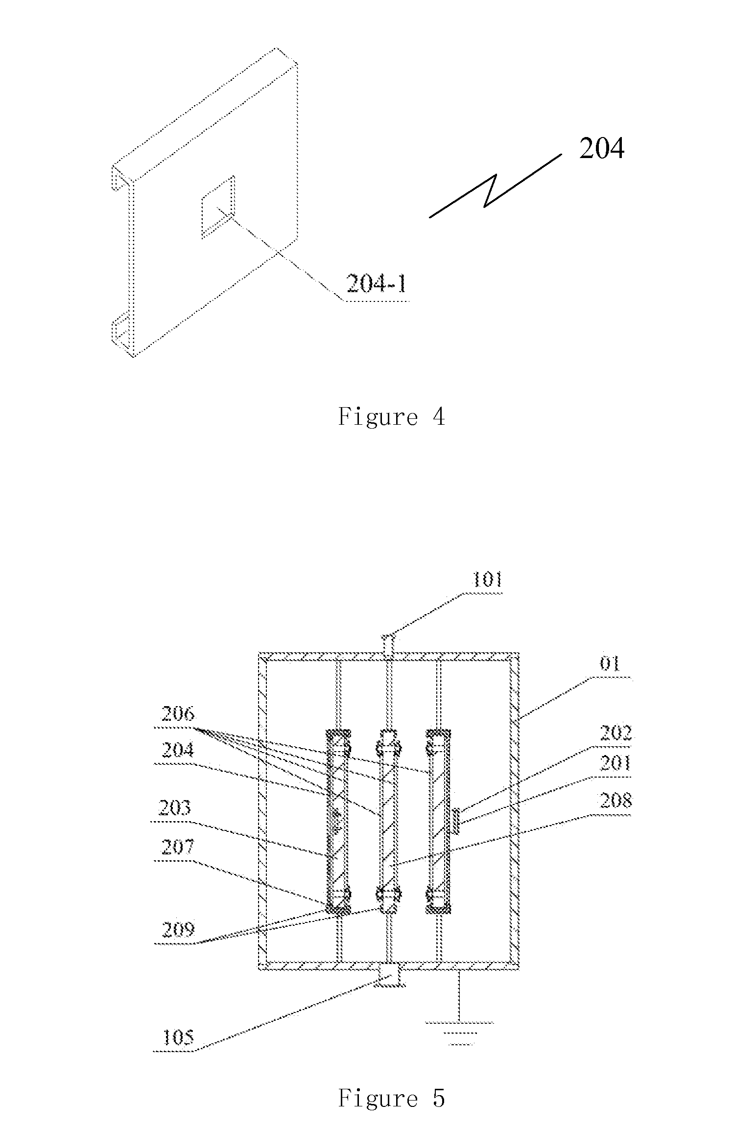
[0032]The principle of this embodiment is illustrated with FIGS. 1-4. As shown, two cathode plates 203 surround one anode plate 208 to form two pairs of electrodes. Four pieces of substrates 206 can be deposited at the same time. More pairs of electrodes can be arranged in an array to improve efficiency of the electrode array.
[0033]The vapor deposition system includes vapor deposition chamber, gas system, electrical power system, vacuum system, heating system, control system, and so on (not all shown). The gas system mainly provides different gases and gas lines for vapor deposition. Electrical power system mainly provides high-frequency or very-high-frequency electrical power source to discharge plasma for film deposition. Vacuum system mainly provides vacuum pumping machines and vacuum pipelines. Heating system mainly supplies heat for vapor deposition chamber. Control system mainly controls the parameters of deposition process. Vapor deposition chamber is the apparatus for r...
embodiment 2
[0038
[0039]The cathode plate has a rectangular feed-in port. The feed-in component has a flat waist as the feed-in belt, one end of which is in a rectangular shape and in surface contact with the feed-in port of the cathode plate.
[0040]The electrode array in FIG. 5 is similar to that in Embodiment 1. A vertical deposition box or reaction chamber is used. Two cathode plates 203 surround one anode plate 208 to form two pairs of electrodes, and 4 glass substrates 206 can be processed. In such a configuration, four substrates can be coated with thin films at the same time. Detailed processes are illustrated as follows:
[0041]a) Placing 4 glass substrates 206 (1640 mm×707 mm×3 mm) with 600-nm transparent conducting thin films in the substrate position in vacuum chamber 01. Film side of the substrate faces outside, while glass side of the substrate faces toward electrode plate.
[0042]b) Filling the vacuum chamber with argon when vacuum reaches 5.0×10⁻⁴ Pa. When the pressure reaches approxim...
embodiment 3
[0051
[0052]The cathode plate has a rectangular feed-in port. The feed-in component has a flat waist as the feed-in belt, one end of which is in a rectangular shape and in surface contact with the feed-in port of the cathode plate.
[0053]The electrode array in FIG. 6 is similar to that in Embodiment 1. A vertical deposition box or reaction chamber is used. Twelve cathode plates 203 and six anode plates 208 form twelve pairs of electrodes, with two cathode plates 203 coupled to or surrounding one anode plate 208 to form two pairs of electrodes, and 24 glass substrates 206 can be processed. In such a configuration, twenty four substrates can be coated with thin films at the same time.
[0054]a) Placing 24 glass substrates 206 (1640 mm×707 mm×3 mm) with 600-nm transparent conducting thin films in 24 substrate position in vacuum chamber 01 arranged from left to right. Film side of the substrate faces outside, while glass side of the substrate faces toward electrode plate.
[0055]b) Filling th...
PUM
| Property | Measurement | Unit |
|---|---|---|
| frequency | aaaaa | aaaaa |
| frequency | aaaaa | aaaaa |
| excitation frequency | aaaaa | aaaaa |
Abstract
Description
Claims
Application Information


