Photomask and near-field exposure method
a near-field exposure and mask technology, applied in the field of masks, can solve the problems of not being directly applied to the near-field mask exposure, shortened wavelength of light source,
- Summary
- Abstract
- Description
- Claims
- Application Information
AI Technical Summary
Benefits of technology
Problems solved by technology
Method used
Image
Examples
embodiment 1
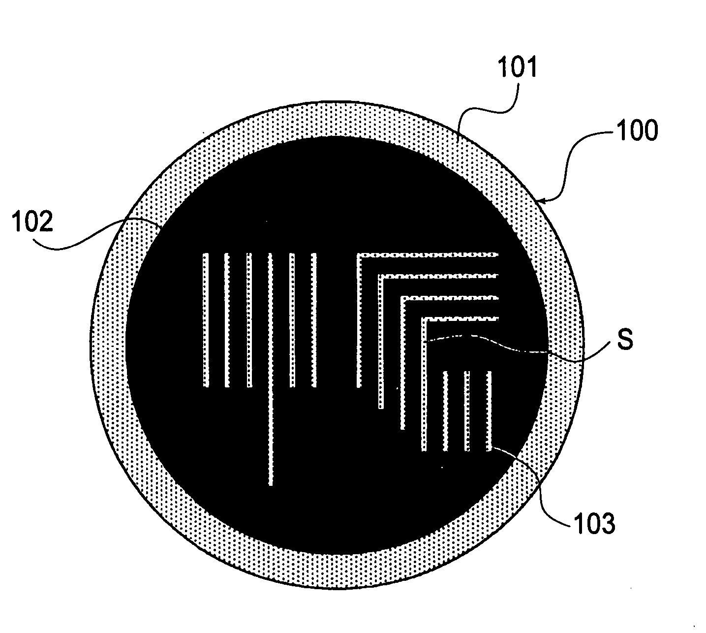
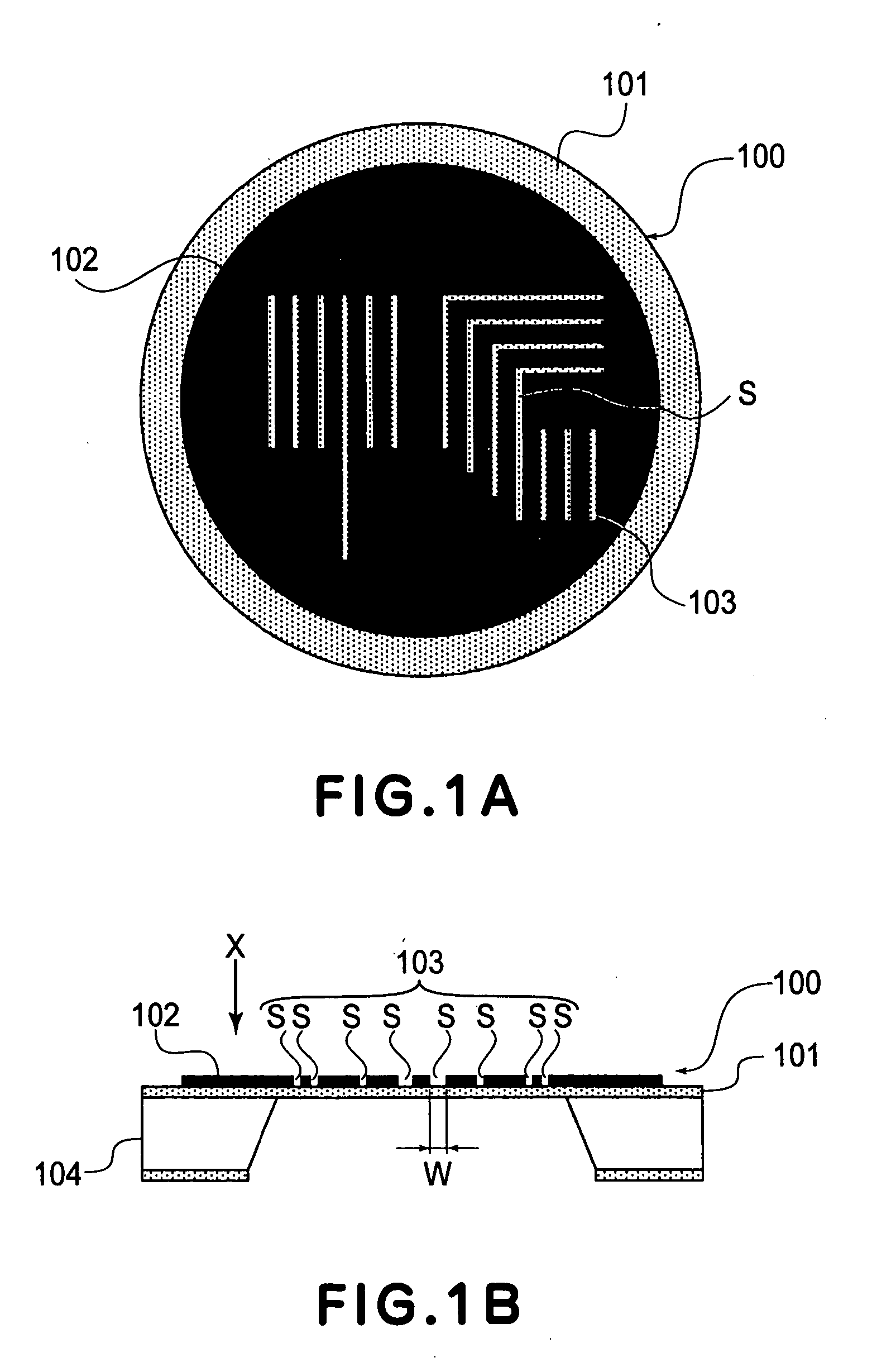
[0025]FIGS. 1A and 1B show a known type photomask 100 for a near-field one-shot exposure process. Specifically, FIG. 1A is a plan view of the photomask 100 as viewed from the front surface side (in a direction of an arrow X in FIG. 1B). FIG. 1B is a longitudinal section of the photomask 100 being mounted to a supporting member 104, the section being taken along the thickness direction thereof.
[0026] As shown in these drawings, the photomask 100 comprises a mask base material 101 and a light blocking film 102 provided on the mask base material 101 (on the front surface thereof).
[0027] The mask base material 101 has a thickness T of 0.1-100 μm, and it is made of a material such as SiN, SiO2 or SiC, for example, having large transmittance with respect to exposure light (to be described later).
[0028] On the other hand, the light blocking film 102 has a thickness t, and it is made of a metal material such as Cr, Al, Au or Ta, for example, having small transmittance with respect to the...
embodiment 2
[0062]FIG. 6 shows another example of photomask 100 to which the present invention is applied. In this embodiment, an auxiliary small opening (correction opening) is additionally provided outside the slit array. It has been confirmed that, with such correction opening means, even at an outermost slit S, the strengthening effect from an adjacent outward opening as described above is available.
[0063] The design conditions were similar to those of FIG. 5, but in this example, outside an array of five slits S having a pitch p of 100 nm, an opening width 40 nm and an opening length of 2,000 nm, there were provided correction openings Sa having an opening width 20 nm and an opening length 2,000 nm. The distance between the center of the correction opening Sa and the center of a slit S, of the five slits S, adjoining the correction opening Sa, was made slightly larger than the pitch p (=100 nm) of the arrayed slits S, and it was equal to 110 nm.
[0064] In this case, since it is undesirabl...
embodiment 3
[0070]FIG. 7 shows a further example of photomask 100 to which the present invention is applied. In this example, additional openings Sb are provided in accordance with the same principle as has been described with reference to FIG. 6.
[0071] In this example, in place of using a slit of smaller opening width as a correction opening, the correction opening Sb consists of an array of very small openings each having the same opening width as that of the slit S of the slit array but having an opening length even smaller than a half of the wavelength.
[0072] The intensity distribution of near-field light provided by such small openings being smaller, in both of lateral size and longitudinal size, than the wavelength would be weak as compared with the intensity distribution of the near-field light to be provided by slit-like opening. Thus, with the method described above, a correction opening Sb that provides a weak strength than the opening of slit array S can be formed.
[0073] The corre...
PUM
| Property | Measurement | Unit |
|---|---|---|
| size | aaaaa | aaaaa |
| thickness | aaaaa | aaaaa |
| thickness | aaaaa | aaaaa |
Abstract
Description
Claims
Application Information


