Apparatus and method of shaping profiles of large-area PECVD electrodes

a technology of pecvd electrodes and apparatus, which is applied in the direction of chemical vapor deposition coating, coating, electric discharge tubes, etc., can solve the problems of adversely affecting the uniformity of plasma and the deposition of substrate, degrading display quality, and uniform deposition properties, etc., to achieve plasma-enhanced chemical vapor deposition

Inactive Publication Date: 2006-01-12
APPLIED MATERIALS INC
View PDF50 Cites 52 Cited by
  • Summary
  • Abstract
  • Description
  • Claims
  • Application Information

AI Technical Summary

Benefits of technology

[0020] A substrate support assembly for supporting a large-area glass substrate in a plasma-enhanced chemical vapor deposition (PECVD) chamber is also provided. In one arrangement, the substrate support assembly first includes a substrate support fabricated from a thermally conductive metal and serving as a lower electrode. The substrate support is fabricated from a material having insufficient strength to support itself under operating conditions. In one embodiment, the substrate support has an appropriately varied thickness to offset anticipated thermally induced planarity changes during substrate processing. In addition, the substrate support assembly includes a base structure for supporting the substrate support. Preferably, the base structure is a lattice-type structure that includes at least one ceramic base plate oriented in a first direction, and at least two ceramic support plates disposed on the at least one base plate and oriented generally transverse to the at least one base plate. Each of the ceramic support plates may have at least one shim disposed on a top surface to offset the nonplanar response of the substrate support under operating conditions. Preferably, the base structure has sufficient strength to rigidly support itself under operating conditions.

Problems solved by technology

Larger sizes can produce non-uniformities in the deposition properties of the plasma which may degrade display quality.
Deformation of the flat substrate may generally include failure of the substrate to maintain a planar, flat profile on the substrate support, such as bowing.
This deformation of the substrate may cause small amounts of gas to become trapped between the substrate and the substrate support, which can adversely affect the uniformity of the plasma and the deposition on the substrate.
In addition, deformation of the substrate may cause a lack of uniform contact between the substrate support and the supported substrate.
In these instances, good physical contact between the substrate and the substrate support may be lost, or may never even be obtained.
Lack of good physical contact with the substrate support may affect the uniformity of the deposition process.
In some instances, fatiguing of the substrate support and supported substrate may cause the substrate to lose a desired orientation to the orientation of a gas diffusion plate, upper electrode, or a gas diffusion plate that also functions as a lower electrode.

Method used


Image

  • Apparatus and method of shaping profiles of large-area PECVD electrodes
  • Apparatus and method of shaping profiles of large-area PECVD electrodes
  • Apparatus and method of shaping profiles of large-area PECVD electrodes

Examples


Embodiment Construction

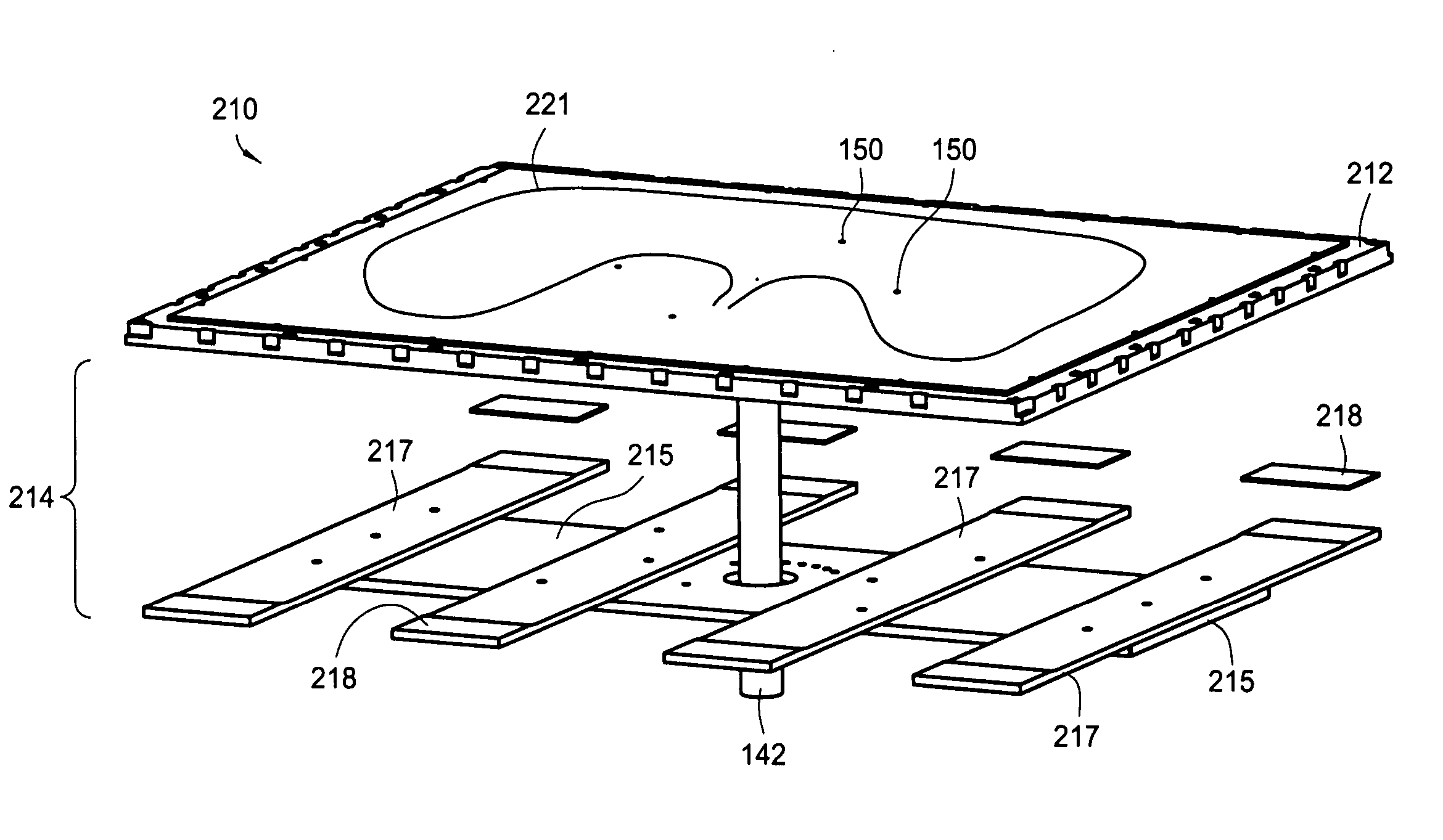
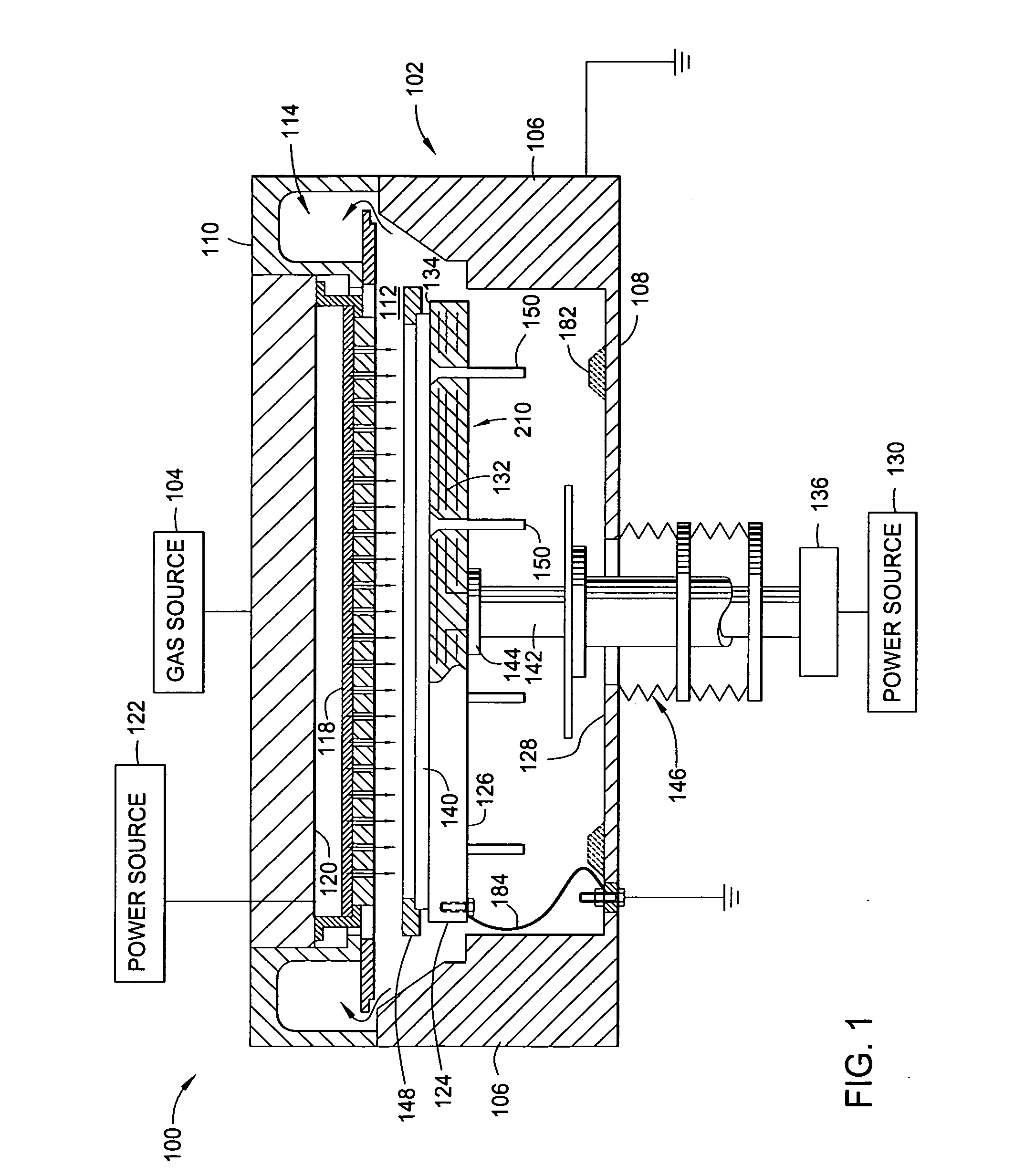
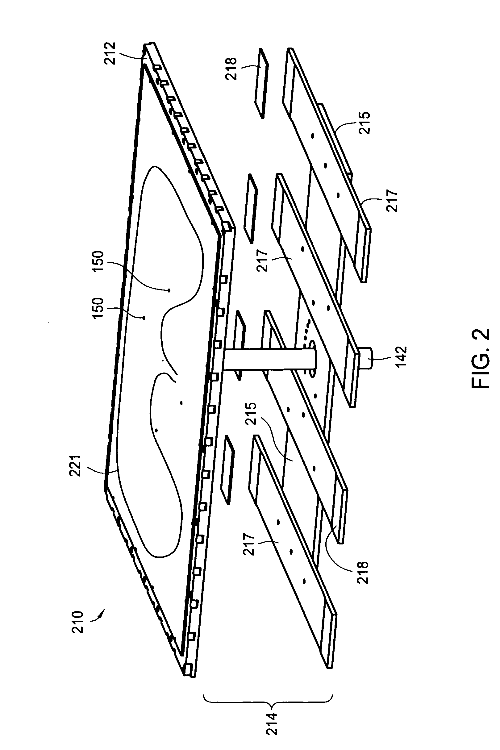
[0033]FIG. 1 is a side, cross-sectional view of one embodiment of a substrate processing chamber 100. The processing chamber 100 is configured to receive a large-area flat substrate 140, and to provide plasma-enhanced chemical vapor deposition on the substrate 140. For purposes of this disclosure, the term “large-area substrate” refers to a substrate having a cross-sectional area of about 1.0 meters2 or larger. In addition, for purposes of this disclosure, the term “plasma-enhanced chemical vapor deposition” (PECVD) refers to any chamber used in the processing of a large area substrate including a plasma etching chamber, a chemical vapor deposition (“CVD”) chamber, a rinse chamber, or other known chamber. In addition, the chamber 100 may be a stand-alone chamber, an in-line chamber, a cluster tool chamber, or some combination or variation thereof.

[0034] The chamber 100 includes a grounded chamber body 102 coupled to a gas source 104 and a power source 122. The chamber body 102 has ...


PUM

PropertyMeasurementUnit
cross-sectional areaaaaaaaaaaa
temperatureaaaaaaaaaa
thicknessaaaaaaaaaa

Abstract

An apparatus and method for shaping profiles of a large-area PECVD electrode is provided. A plasma-enhanced CVD chamber for processing a large-area substrate is first provided. The chamber includes a lower electrode that supports a large area substrate. The lower electrode is shaped to selectively conform the supported substrate in a selected orientation under operating conditions. The orientation may be either planar or nonplanar. The substrate complies with the shape of the electrode so the substrate is substantially parallel to an upper electrode in the chamber, and / or to a gas diffusion plate in the chamber. The lower electrode comprises a substrate support fabricated from a material of insufficient strength to support itself at operating temperatures and pressure in the chamber. The shape of the substrate support is adjusted by modifying the dimensions and / or planarity of a supporting base structure, and / or by appropriately varying the thickness of the substrate support.

Description

CROSS REFERENCE TO RELATED APPLICATIONS [0001] This application claims priority to U.S. Provisional Patent Application No. 60 / 587,173, filed Jul. 12, 2004.BACKGROUND OF THE INVENTION [0002] 1. Field of the Invention [0003] Embodiments of the present invention generally relate to substrate processing methods, such as methods for processing flat-panel displays. Embodiments of the present invention also generally relate to a processing apparatus for processing flat panel displays. In addition, the invention relates to a plasma-enhanced CVD processing chamber. [0004] 2. Description of the Related Art [0005] Flat panel displays are commonly used for computer screens, television monitors, cell phone displays, personal digital assistants, and other electronic equipment. Flat panel displays employ an active matrix of electronic devices, such as thin film transistors, or TFT's. The electronic devices are conventionally made on large flat substrates referred to as flat panel substrates. Gener...

Claims


Application Information

Patent Timeline
Patent Type & Authority Applications(United States)
IPC IPC(8): C23C16/00C23F1/00
CPCC23C16/4583H01J2237/3325H01J37/3244
Inventor WHITE, JOHN M.BEER, EMANUELCHANG, WEITINER, ROBIN L.CHOI, SOO YOUNG
Owner APPLIED MATERIALS INC
Why Eureka
Try Eureka