Thin film solar cell and manufacturing method thereof

a technology manufacturing methods, applied in semiconductor/solid-state device manufacturing, electrical apparatus, semiconductors, etc., can solve the problems of not disclosed the integration of p-type tco for manufacturing thin film solar cells, complicated production of p-type tco, and limited mass production of thin film solar cells. , to achieve the effect of preventing reducing the damage to the tco surface, and reducing the damage to the

Inactive Publication Date: 2011-06-30
NEXPOWER TECH
View PDF3 Cites 4 Cited by
  • Summary
  • Abstract
  • Description
  • Claims
  • Application Information

AI Technical Summary

Benefits of technology

Therefore, it is a primary objective of the invention to propose a thin film solar cell that has the p-type interlayer having wok function of 5˜7 eV and disposed between the front electrode layer and the absorber layer, so as to enhance the open-circuit voltage of the thin film solar cell.
Therefore, it is a primary objective of the invention is to propose a method of manufacturing the thin film solar cell where the p-type interlayer is formed on the front electrode layer so as to restrain the damage to the TCO surface, and further to prevent damage to the TCO surface from hydrogen plasma generated by plasma-enhanced chemical vapor deposition (PECVD) used for manufacturing the absorber layer.
it is a another objective of the invention is to propose a method of manufacturing the thin film solar cell where the interlayer is formed on the absorber layer by doping group III element into a zinc oxide of the front electrode layer, and thus the process of producing the p-type TCO is simplified so as to improve the mass production of thin film solar cell.

Problems solved by technology

However, the process of producing the p-type TCO is too complicated so that mass production of thin film solar cell is limited.
Nevertheless, the aforementioned prior arts have not disclosed the way to integrating the p-type TCO for manufacturing the thin film solar cell.

Method used


Image

  • Thin film solar cell and manufacturing method thereof
  • Thin film solar cell and manufacturing method thereof
  • Thin film solar cell and manufacturing method thereof

Examples


Embodiment Construction

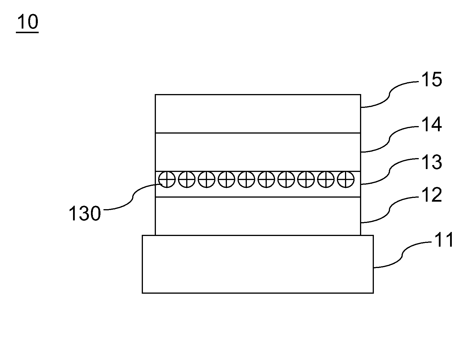
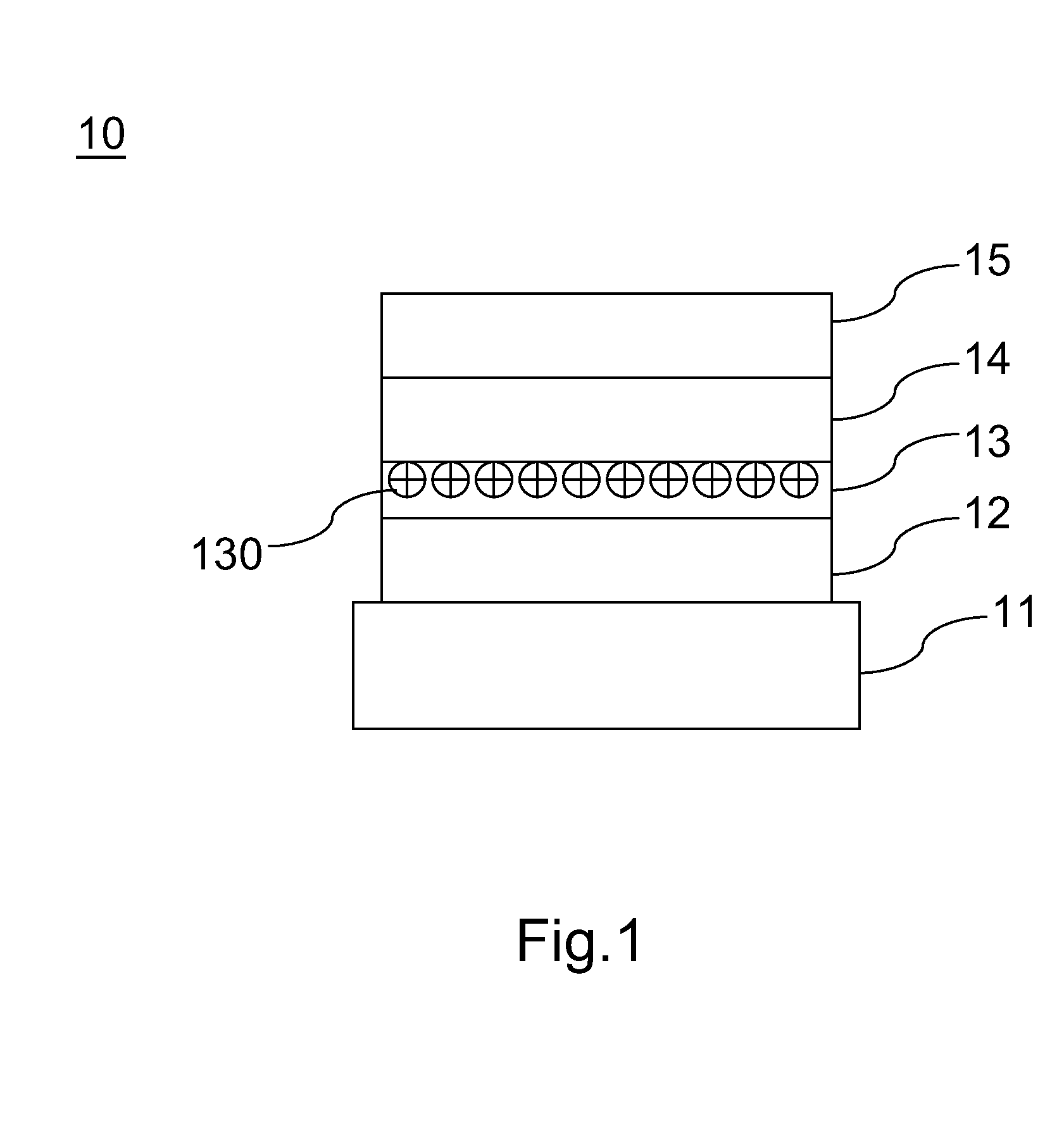
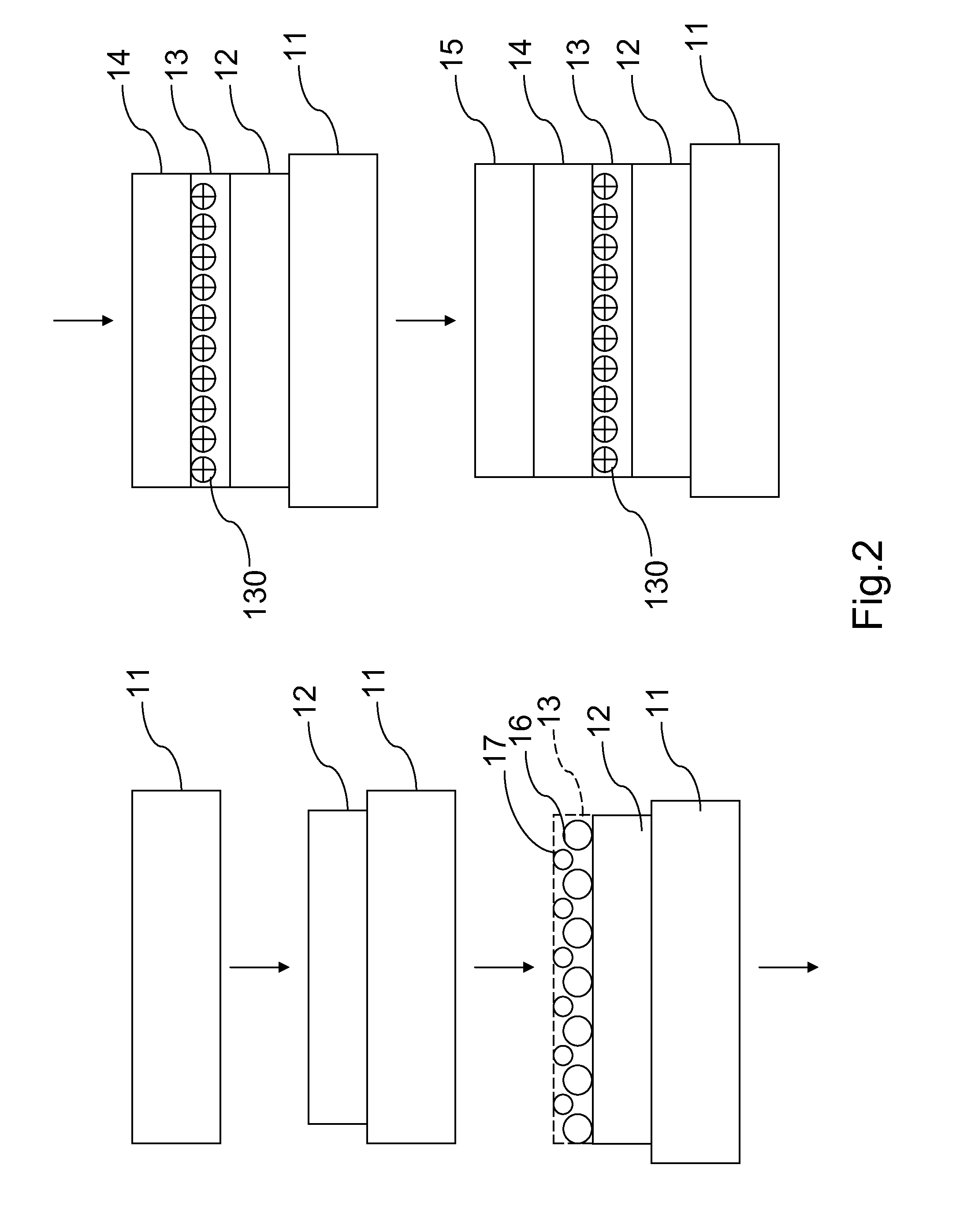
A thin film solar cell and manufacturing method thereof has been disclosed in the invention; wherein the principles of photoelectric conversion employed in solar cell may be easily comprehended by those of ordinary skill in relevant technical fields, and thus will not be further described hereafter. Meanwhile, it should be noted that the drawings referred to in the following paragraphs only serve the purpose of illustrating structures related to the characteristics of the disclosure, and are not necessarily drawn according to actual scales and sizes of the disclosed objects.

Refer to FIG. 1, which is a sectional view that show a thin film solar cell according to a first preferred embodiment of the invention. The thin film solar cell 10 comprises a substrate 11, a front electrode layer 12, an absorber layer 14 and a rear electrode layer 15 stacked in such sequence, wherein the front electrode layer 12 is formed by means of doping group III element into a zinc oxide. The thin-film sola...


PUM


Abstract

The present invention relates to a thin film solar cell and manufacturing method thereof. The thin film solar cell comprises a substrate, a front electrode layer, an absorber layer and a rear electrode layer stacked in such sequence, wherein the front electrode layer is formed by doping group III element into a zinc oxide. The thin-film solar cell further comprise an interlayer disposed between the front electrode layer and the absorber layer wherein the interlayer has p-type holes formed by introducing nitrogen-based gas having Argon (Ar) as a carrier gas interacted with the group III element by using PECVD or thermal treatment, implementation and diffusion on the front electrode layer surface so that the concentration of nitrogen atoms in the interlayer is greater than 1015 / cm3.

Description

FIELD OF THE INVENTIONThe invention relates to a thin film solar cell and manufacturing method thereof, and more particularly to the thin film solar cell and manufacturing method thereof using nitrogen-based gas for TCO surface treatment.DESCRIPTION OF PRIOR ARTA conventional thin film solar cell comprises a substrate, a front electrode layer, an absorber layer and a back electrode layer. Particularly, the front electrode layer uses transparent conductive oxide (TCO) as its material. For the sake of obtaining better open-circuit voltage and preventing damage to the TCO surface from hydrogen plasma generated by plasma-enhanced chemical vapor deposition (PECVD) used for manufacturing the absorber layer. Conventionally, a thin film of p-type TCO is usually formed on the glass or n-type TCO as a protection layer so as to restrain the damage to the TCO surface. However, the process of producing the p-type TCO is too complicated so that mass production of thin film solar cell is limited.A...

Claims


Application Information

Patent Timeline
Patent Type & Authority Applications(United States)
IPC IPC(8): H01L31/0304H01L31/18
CPCY02E10/50H01L31/0392H01L31/022466
Inventor YEH, CHIH-HUNGLU, WEI-LUNHOU, BING-YILAI, KUANG-CHIEH
Owner NEXPOWER TECH
Why Eureka
Try Eureka