Method for fabricating a tunneling field-effect transistor

a tunneling field-effect transistor and tunneling technology, which is applied in the direction of semiconductor devices, diodes, electrical devices, etc., can solve the problems of reducing the device dimension, restricting the device further, and reducing the requirements of the photolithography process for fabricating a planar tfet, so as to facilitate the fabrication of a planar tfet device with stable and reliable characteristics, and reduce the requirements of the photolithography process. , the effect o

Active Publication Date: 2012-10-16
SEMICON MFG INT (SHANGHAI) CORP +1
View PDF5 Cites 5 Cited by
  • Summary
  • Abstract
  • Description
  • Claims
  • Application Information

AI Technical Summary

Benefits of technology

[0011]4) depositing the second hard dielectric to cover the drain region, and a CMP process is carried out on the second hard dielectric by using the upper surface of the first hard dielectric as the stop layer, thereby forming a hard mask over the drain region to protect the drain region;
[0013]6) depositing the second hard dielectric to cover the source region, and a CMP process is carried out on the second hard dielectric by using the upper surface of the first hard dielectric as the stop layer, thereby forming a hard mask over the source region to protect the source region;
[0018]In the above steps 4) and 6), chemical vapor deposition is employed to deposit the second hard dielectric; and preferably, a plasma-enhanced chemical vapor deposition (PECVD) is employed to reduce diffusion of impurities during deposition.
[0021]Since the doping types of the source region and the drain region of the tunneling field-effect transistor (TFET) are different, two times of photolithography process are needed in the traditional method for fabricating a planar TFET to define the source region and the drain region of the device, and thus requirements on the photolithography process are very strict in such a non-self-aligned fabrication procedure. However, in the method for self-alignedly fabricating a planar TFET according to the invention, the requirements on the photolithography processes for fabricating a planar TFET may be lowered. In the method of the invention, the source and drain regions of the TFET are not defined by photolithography directly; instead, they are defined by the dielectric films over the active region and on both sides of the gate, and the influence due to the alignment deviation among the three times of photolithography processes for defining the channel region, the source and drain regions may be eliminated by etching the dielectric films over the source and drain regions by wet etching. Therefore, based on this process, a planar TFET can be fabricated self-alignedly, thereby the rigid requirements on the alignment deviation of photolithography during the fabrication procedure of the planar TFET is alleviated, which facilitates to fabricate a planar TFET device with stable and reliable characteristics.

Problems solved by technology

However, when the device dimension entered the sub-100 nm regime, the impact of short channel effects such as drain-induced barrier lowering (DIBL), shift of threshold voltage, off-state leakage current increasing and sub-threshold slope (SS) degradation are becoming more and more severe, which restricts the device dimension from further downscaling.
Thus it is very difficult to fabricate TFET based on the self-aligned planar fabrication process of conventional MOSFET.
Particularly, when the device has a short channel length, the unstability of device characteristics caused by the alignment deviation of the photolithography becomes more severe.
However, for a TFET fabricated by the above methods, overlap between the gate region and the source (or drain) region is very large, which may increase the parasitic capacitance and gate leakage; moreover, the compatibility between the TFET having a vertical structure and the existing planar ultra-large scale integrated circuit is poor, which is unfavorable for an integration of the TFET and the traditional planar MOSFET.

Method used


Image

  • Method for fabricating a tunneling field-effect transistor
  • Method for fabricating a tunneling field-effect transistor
  • Method for fabricating a tunneling field-effect transistor

Examples


Embodiment Construction

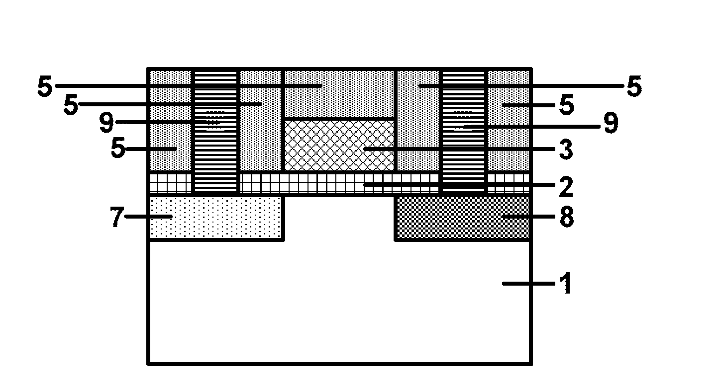
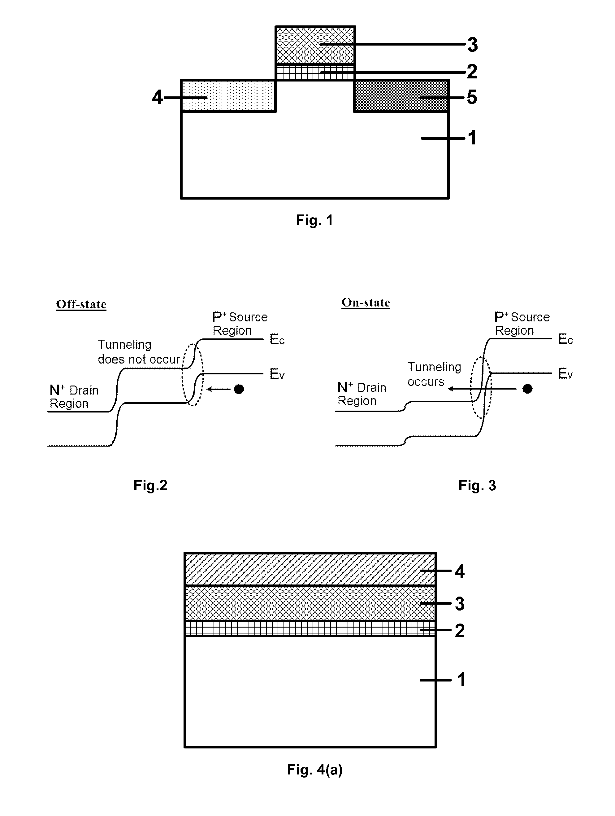
[0029]The invention will be described in detail in conjunction with the drawings and specific embodiments, and a process for self-alignedly fabricating a TFET according to the invention will be provided specifically; however, it is not intended to be interpreted as limiting the scope of the invention in any way.

[0030]A tunneling field-effect transistor is fabricated in the following steps:

[0031]1) providing a substrate which comprises a bulk silicon substrate, and defining an active region using shallow trench isolation (STI);

[0032]2) forming silicon oxide, i.e., a gate dielectric layer, with a thickness of 50 Å, by gate-oxide oxidation;

[0033]3) depositing polysilicon with a thickness of 2000 Å on the gate dielectric layer by low pressure chemical vapor deposition (LPCVD);

[0034]4) As implantation is carried out with respect to the polysilicon, with an implantation energy of 50 Key and a dosage of 4×10¹⁵ / m2;

[0035]5) depositing silicon nitride with a thickness of 2000 Å on the polysi...


PUM


Abstract

The present invention discloses a method for self-alignedly fabricating tunneling field-effect transistor (TFET) based on planar process, thereby lowering requirements on a photolithography process for fabricating the planar TFET. In the method, the source region and the drain region of the TFET are not directly defined by photolithography; rather, they are defined by another dielectric film which locates over an active region and on both sides of the gate and which is different from the dielectric film that defines the channel region. The influence due to the alignment deviation among three times of photolithography process for defining the channel region, the source and the drain regions may be eliminated by selectively removing the dielectric film over the source and drain regions by wet etching. Therefore, a planar TFET may be fabricated self-alignedly based on this process, thereby the rigid requirements on the alignment deviation of the photolithography during the fabrication procedure of a planar TFET is alleviated, which facilitates to fabricate a planar TFET device with stable and reliable characteristics.

Description

FIELD OF THE INVENTION[0001]The present invention relates to a process for fabricating a semiconductor device, and in particular, to a method for fabricating a tunneling field-effect transistor (TFET).BACKGROUND OF THE INVENTION[0002]Ultra-large scale integrated circuits technology has been driven by the scaling down of CMOS device to improve the performance, as well as to reduce the cost. However, when the device dimension entered the sub-100 nm regime, the impact of short channel effects such as drain-induced barrier lowering (DIBL), shift of threshold voltage, off-state leakage current increasing and sub-threshold slope (SS) degradation are becoming more and more severe, which restricts the device dimension from further downscaling. Besides adopting novel device structures and new materials, the impact of the short channel effects of the MOSFET can be reduced by changing the operating mechanism of field effect transistor, for example, by employing a tunneling field-effect transis...

Claims


Application Information

Patent Timeline
Patent Type & Authority Patents(United States)
IPC IPC(8): H01L21/336
CPCH01L29/66356H01L29/7391
Inventor HUANG, RUAI, YUJIEHAO, ZHIHUAFAN, CHUNHUIPU, SHUANGSHUANGWANG, RUNSHENGYUN, QUANXIN
Owner SEMICON MFG INT (SHANGHAI) CORP
Why Eureka
Try Eureka