Nitride-based compound semiconductor light emitting device and fabricating method thereof

a light-emitting device and compound semiconductor technology, which is applied in the direction of semiconductor devices, basic electric elements, electrical equipment, etc., can solve the problems of sapphire substrate removal, hindering the formation of light-emitting devices, and conductive substrates that may peel off from the ohmic electrode, etc., and achieve good adhesion and high reliability.

Active Publication Date: 2006-01-12
SHARP KK
View PDF28 Cites 29 Cited by
  • Summary
  • Abstract
  • Description
  • Claims
  • Application Information

AI Technical Summary

Benefits of technology

[0012] The present invention has been made to solve the above-described problems of the conventional techniques, and an object of the present invention is to provide a highly rel

Problems solved by technology

With such a technique, however, the conductive substrate may peel off from the ohmic electrode due to poor adhesion therebetween.
If the conductive substrate and the ohmic electrode are separated from each other completely, it is not possible to remove a sapphire substrate, hindering formation of a light emitting device.
If they are partially separated from each other, flow of the current from the gallium nitride-based semiconductor layer to the conductive substrate will be difficult, leading to an increase of operating voltage, thereby causing degradation in reliability of the light emitting device.
Further, the partially

Method used


Image

  • Nitride-based compound semiconductor light emitting device and fabricating method thereof
  • Nitride-based compound semiconductor light emitting device and fabricating method thereof
  • Nitride-based compound semiconductor light emitting device and fabricating method thereof

Examples


example 1

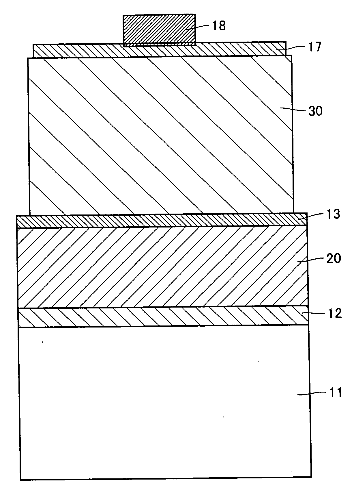
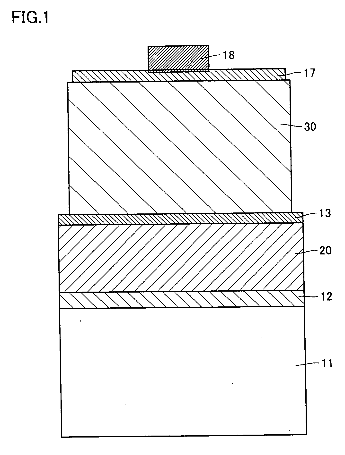
[0061] On a Si substrate serving as support substrate 11, a Ti (15 nm) / Al (150 nm) layer serving as first ohmic electrode 12 and an Au (3 μm) layer serving as first bonding metal layer 21 were formed in this order by EB evaporation.

[0062] Next, on a sapphire substrate serving as substrate 35, buffer layer 36, N-type nitride-based compound semiconductor layer 31, light emitting layer 32, and P-type nitride-based compound semiconductor layer 33 were formed successively by MOCVD. Specifically, a GaN buffer layer serving as buffer layer 36 was formed to a thickness of 20 nm, N-type nitride-based compound semiconductor layer 31 was formed to a thickness of 7 μm, a multi-quantum well (MQW) light emitting layer serving as light emitting layer 32 was formed to a thickness of 50 nm, and P-type nitride-based compound semiconductor layer 33 was formed to a thickness of 200 nm, successively in this order.

[0063] Next, on P-type nitride-based compound semiconductor layer 33, second ohmic electr...

example 2

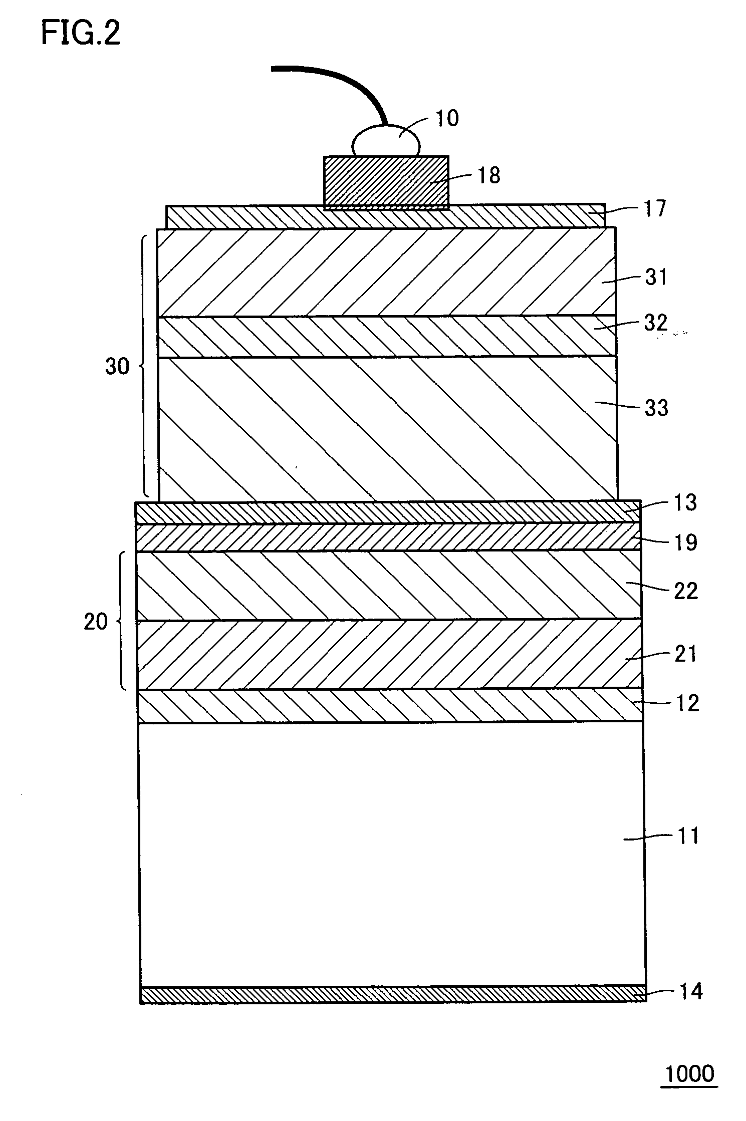
[0069] On a CuW substrate serving as support substrate 11, a Ti (15 nm) / Al (150 nm) layer serving as first ohmic electrode 12 and an Au (3 μm) layer serving as first bonding metal layer 21 were formed in this order by EB evaporation.

[0070] Next, on a sapphire substrate serving as substrate 35, buffer layer 36, N-type nitride-based compound semiconductor layer 31, light emitting layer 32, and P-type nitride-based compound semiconductor layer 33 were formed successively, using MOCVD. Specifically, a GaN buffer layer serving as buffer layer 36 was formed to a thickness of 20 nm, N-type nitride-based compound semiconductor layer 31 was formed to a thickness of 5 μm, an MQW light emitting layer serving as light emitting layer 32 was formed to a thickness of 50 nm, and P-type nitride-based compound semiconductor layer 33 was formed to a thickness of 200 nm, successively in this order.

[0071] Next, second ohmic electrode 13, reflecting metal layer 19, barrier metal layer 15 and second bon...


PUM


Abstract

The nitride-based compound semiconductor light emitting device includes a first ohmic electrode, a bonding metal layer, a second ohmic electrode, a nitride-based compound semiconductor layer, and a transparent electrode stacked in this order on a support substrate, and further includes an ohmic electrode formed on a back side of the support substrate.

Description

[0001] This nonprovisional application is based on Japanese Patent Application No. 2004-201743 filed with the Japan Patent Office on Jul. 8, 2004, the entire contents of which are hereby incorporated by reference. BACKGROUND OF THE INVENTION [0002] 1. Field of the Invention [0003] The present invention relates to a nitride-based compound semiconductor light emitting device capable of emitting light in the blue to ultraviolet range, and a fabricating method thereof. More particularly, the present invention relates to a nitride-based compound semiconductor light emitting device having a conductive substrate bonded thereto and a fabricating method thereof. [0004] 2. Description of the Background Art [0005] A nitride-based compound semiconductor, represented by InxGayAlzN (x+y+z=1, 0≦x<1, 0<y≦1, 0≦z<1), for example, has a large energy bandgap and high thermal stability, and allows control of the bandgap width by adjusting composition thereof. Accordingly, the nitride-based comp...

Claims


Application Information

Patent Timeline
IPC IPC(8): H01L29/22H01L33/00H01L33/32
CPCH01L33/0079H01L33/32H01L2224/48463H01L2924/12041H01L2924/01322H01L2224/45144H01L2924/00014H01L2924/00H01L33/0093
Inventor HATA, TOSHIO
Owner SHARP KK
Why Eureka
Try Eureka