Semiconductor devices having a metal-insulator-metal capacitor and methods of forming the same

a technology of metal-insulator and capacitor, which is applied in the direction of semiconductor devices, capacitors, electrical devices, etc., can solve the problems of difficult polishing of noble metal layers, affecting the yield of semiconductor devices, and affecting the quality of semiconductor devices, so as to achieve the effect of preventing defects

Active Publication Date: 2006-01-12
SAMSUNG ELECTRONICS CO LTD
View PDF11 Cites 40 Cited by
  • Summary
  • Abstract
  • Description
  • Claims
  • Application Information

AI Technical Summary

Benefits of technology

[0011] An aspect of the present invention is to provide a semiconductor device having an MIM capacitor capable of

Problems solved by technology

However, it is very difficult to polish noble metal layers including the platinum layer 6 using chemical mechanical polishing

Method used


Image

  • Semiconductor devices having a metal-insulator-metal capacitor and methods of forming the same
  • Semiconductor devices having a metal-insulator-metal capacitor and methods of forming the same
  • Semiconductor devices having a metal-insulator-metal capacitor and methods of forming the same

Examples


Embodiment Construction

[0020] Preferred embodiments of the present invention will be described below in more detail with reference to the accompanying drawings. The present invention may, however, be embodied in different forms and should not be constructed as limited to the embodiments set forth herein. Rather, these embodiments are provided so that this disclosure will be thorough and complete, and will fully convey the scope of the invention to those skilled in the art. Like numerals refer to like elements throughout the specification.

[0021] Hereinafter, it will be described about an exemplary embodiment of the present invention in conjunction with the accompanying drawings.

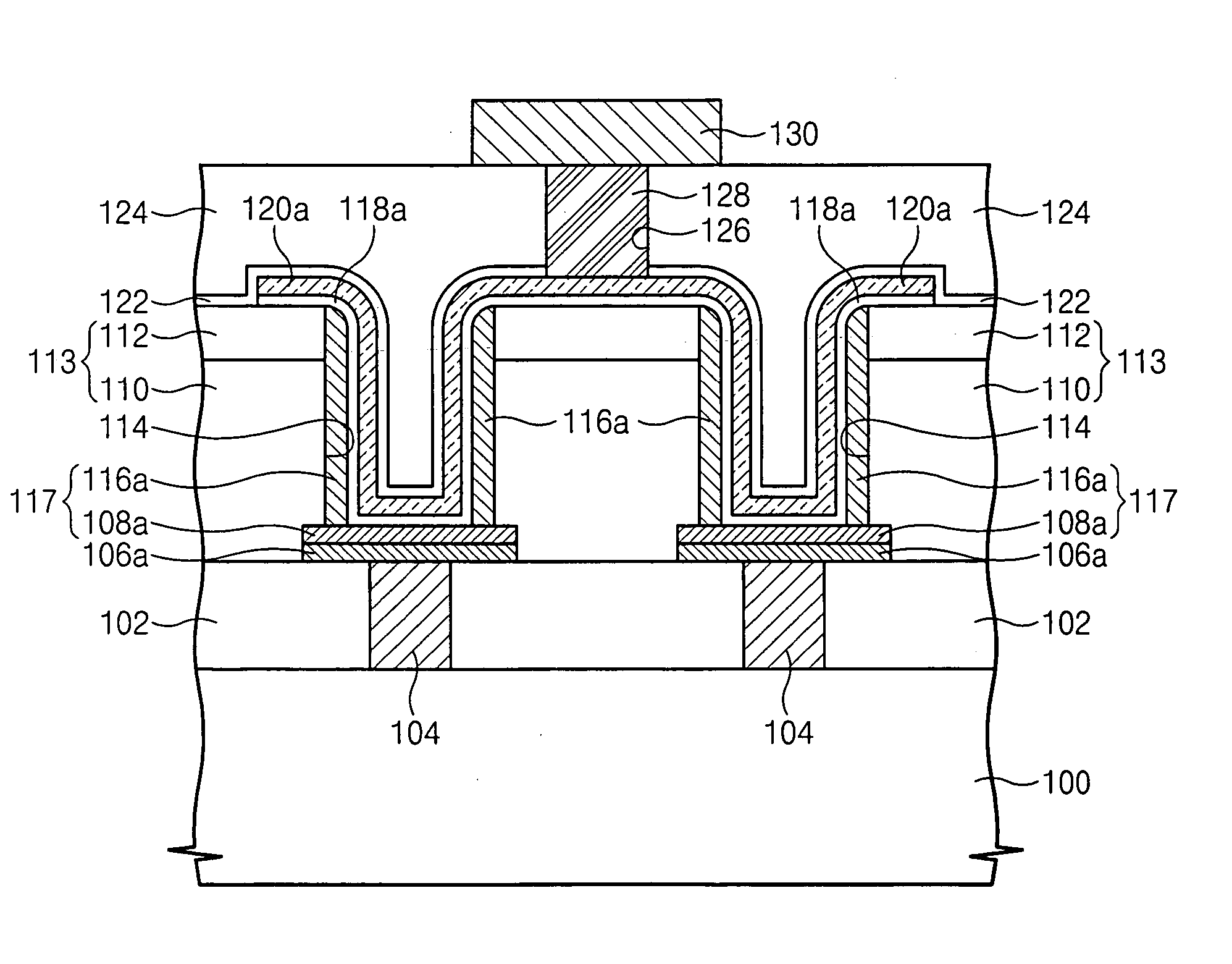
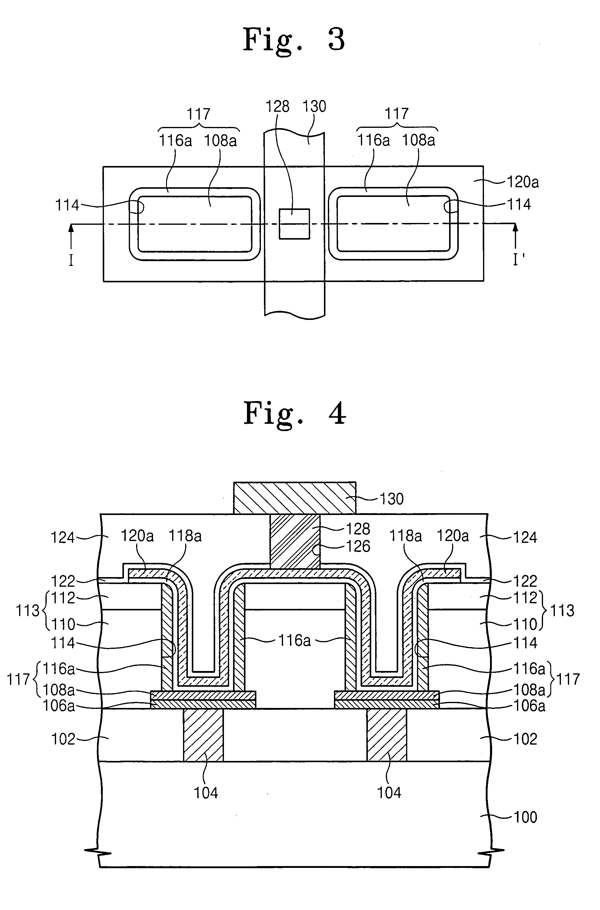
[0022]FIG. 3 is a top plan view showing a semiconductor device having an MIM capacitor and FIG. 4 is a cross-sectional view taken along a line I-I′ in FIG. 3.

[0023] Referring to FIGS. 3 and 4, a lower interlayer insulation layer 102 is disposed on a semiconductor substrate 100 (hereinafter, referred to as ‘a substrate’) and a con...


PUM


Abstract

A semiconductor device having an MIM capacitor and a method of forming the same are provided. A lower electrode includes a plate electrode and a sidewall electrode. The plate electrode is formed by a patterning process preferably including a plasma anisotropic etching. The sidewall electrode is formed like a spacer on an inner sidewall of an opening exposing the plate electrode by a plasma entire surface anisotropic etching.

Description

CROSS-REFERENCE TO RELATED APPLICATIONS [0001] This U.S. non-provisional patent application claims priority under 35 U.S.C. § 119 of Korean Patent Application 2004-54049 filed on Jul. 12, 2004, the entire contents of which are hereby incorporated by reference.BACKGROUND OF THE INVENTION [0002] The present invention relates to a semiconductor device and a method of forming the same and specifically to a semiconductor device including a Metal-Insulator-Metal (MIM) capacitor and a method of forming the same. [0003] A semiconductor capacitor has been widely used as a data storage of unit cells in a DRAM device, a ferroelectric memory device, etc. because of its characteristic of storing electrons. Conventionally, the capacitor includes upper and lower electrodes and a dielectric layer intervening between the upper and lower electrodes. As a capacity of the capacitor increases, the capacitor stores more electrons. [0004] Electrodes of an MIM capacitor of a semiconductor device are formed...

Claims


Application Information

Patent Timeline
IPC IPC(8): H01L27/108
CPCH01L27/10852H01L27/11502H01L27/11507H01L28/91H01L28/65H01L28/75H01L28/55H10B12/033H10B53/30H10B53/00H01L27/04H01L21/283
Inventor KIM, HYUN-HOJOO, HEUNG-JINKIM, KI-NAM
Owner SAMSUNG ELECTRONICS CO LTD
Why Eureka
Try Eureka