Liquid crystal display panel with built-in driving circuit

a technology of driving circuit and liquid crystal display panel, which is applied in the field of liquid crystal display panel having a built-in driving circuit, can solve the problems of product standardization and limit the area that can be enlarged within the circuit area, and achieve the effect of prolonging the life of the liquid crystal display panel and reducing the distortion of the scanning pulse waveform

Inactive Publication Date: 2006-01-12
LG DISPLAY CO LTD
View PDF3 Cites 107 Cited by
  • Summary
  • Abstract
  • Description
  • Claims
  • Application Information

AI Technical Summary

Benefits of technology

[0020] An object of the present invention to provide a driving circuit that reduces a distortion of a scanning pulse waveform in a liquid crystal display panel.
[0021] Another object of the present invention is to provide a driving circuit that prolongs the life of a liquid crystal display panel.

Problems solved by technology

However, product standardization limits how much the circuit area can be enlarged within the non-display area.

Method used


Image

  • Liquid crystal display panel with built-in driving circuit
  • Liquid crystal display panel with built-in driving circuit
  • Liquid crystal display panel with built-in driving circuit

Examples


first embodiment

[0048]FIG. 7 is a schematic plan view of an exemplary portion of a thin film transistor substrate of a liquid crystal display panel with a built-in gate driving circuit according to the present invention. Referring to FIG. 7, a thin film transistor substrate includes a display area 74, and odd and even gate driving circuits 70o and 70e built in a non-display area at each side of the display area 74. The display area 74 is provided with gate lines G and data lines D crossing each other. Crossings of the gate lines G and the data lines G define pixel regions in the display area 74. A thin film transistor TFT is connected at a crossing of one of the gate lines G and one of the data lines D. Liquid crystal cells (not shown) are provided in each pixel region. A pixel electrode 76 of the liquid crystal cell in each pixel region is connected to the corresponding thin film transistor TFT in that pixel region. The pixel regions, and the liquid crystal cells within the pixel regions, are arra...

second embodiment

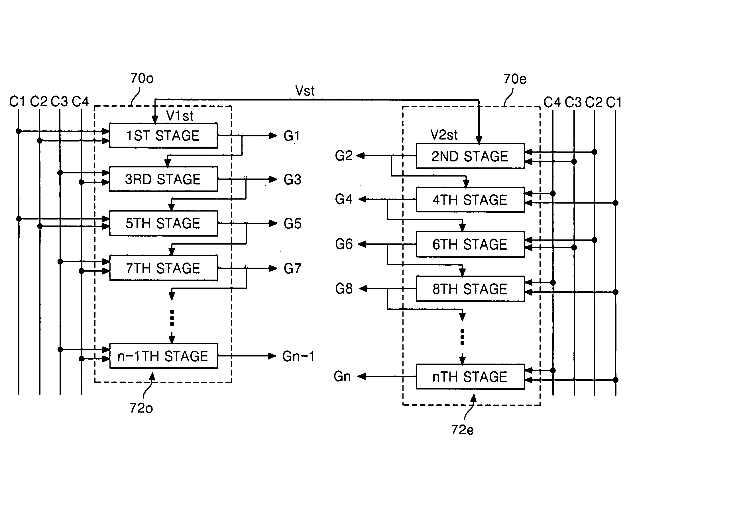
[0051]FIG. 9 is a schematic view for a method of driving odd and even gate driving circuits according to the present invention. Referring to FIG. 9, the odd driving circuit 700 includes 1st, 3rd, 5th, (n−1)-th odd stages. The even driving circuit 70e includes 2nd, 4th, 6th, . . . , n-th even stages. Each of the 2nd, 4th, 6th, . . . , and n-th even stages from the even driving circuit 70e receives an input scanning pulse as a start pulse from the preceding 1st, 3rd, 5th, . . . , or (n−1)-th odd stage, respectively, and shifts it sequentially, thereby driving the even gate lines G2, G4, G4, . . . , and Gn. On the other hand, each of the 1st, 3rd, 5th, . . . , and (n−1)-th odd stages from the odd driving circuit 70o receives an input scanning pulse as a start pulse from the preceding 2nd, 4th, 6th, . . . , or n-th even stage, respectively, and shifts it sequentially, thereby driving the odd gate lines G1, G3, G5, . . . , and Gn−1.

[0052] The first odd stage 1st applies a scanning pulse ...

fourth embodiment

[0063]FIG. 14 is a schematic plan view of an exemplary portion of a thin film transistor substrate of a liquid crystal display panel with a built-in gate driving circuit according to the present invention. Referring to FIG. 14, a thin film transistor substrate includes a display area 144, and odd and even gate driving circuits 140o and 140e built in a non-display area at each side of the display area 144. The display area 144 is provided with an n-number of gate lines G and an m-number of data lines D crossing each other. As an example, the number n of gate lines is equal to m / 2, that is half of the m-number of data lines D. Crossings of the gate lines G and the data lines G define pixel regions in the display area 144. A thin film transistor TFT is connected at a crossing of one of the gate lines G and one of the data lines D. Liquid crystal cells (not shown) are provided in each pixel region. A pixel electrode 146 of the liquid crystal cell in each pixel region is connected to the...


PUM


Abstract

A liquid crystal display panel includes liquid crystal cells forming a matrix in a display area of the liquid crystal display panel; odd and even gate driving circuits provided at an outer area of the display area, the display area being positioned between the odd and even gate driving circuits, the odd driving circuit including a plurality of odd stages, the even driving circuit including a plurality of even stages; a plurality of gate lines, including even gate lines and odd gate lines in the liquid crystal cell matrix, the odd gate lines being driven by the odd driving circuit, and the even gate lines being driven by the even driving circuit, wherein a pitch of each of the odd stages and the even stages corresponds to size larger than a pitch of the liquid crystal cell.

Description

[0001] This application claims the benefit of Korean Patent Application Nos. 10-2004-38888 filed in Korea on May 31, 2004, and 10-2004-73106 filed in Korea on Sep. 13, 2004, both of which are hereby incorporated by reference in their entirety. BACKGROUND OF THE INVENTION [0002] 1. Field of the Invention [0003] This invention relates to a liquid crystal display, and more particularly to a liquid crystal display panel having a built-in driving circuit. [0004] 2. Description of the Related Art [0005] Generally, a liquid crystal display (LCD) device can be used as a display monitor for a television and a computer. In an LCD device, light transmittance of a liquid crystal is controlled using an electric field to thereby display a picture. To this end, the LCD includes a liquid crystal display panel having liquid crystal cells arranged in a matrix type. A driving circuit is provided for driving the liquid crystal display panel. [0006]FIG. 1 is a block circuit diagram showing a configurati...

Claims


Application Information

Patent Timeline
Patent Type & Authority Applications(United States)
IPC IPC(8): G09G3/36
CPCG09G3/3648G11C19/28G09G2300/0426G09G3/3677G02F1/133
Inventor KIM, BINNYOON, SOO YOUNG
Owner LG DISPLAY CO LTD
Why Eureka
Try Eureka