Image sensor

a technology of image sensor and pixel, applied in the field of image sensor, can solve the problems of image quality deterioration and defective pixel flickering, and achieve the effect of suppressing an erroneous detection

Active Publication Date: 2006-01-12
SONY SEMICON SOLUTIONS CORP
View PDF11 Cites 163 Cited by
  • Summary
  • Abstract
  • Description
  • Claims
  • Application Information

AI Technical Summary

Benefits of technology

[0018] According to the image sensor, the defective pixel detection circuit adjusts the detection accuracy of the defective pixel detection in accordance with the exposure condition of the pixel unit. Therefore, the image sensor is advantageous in suppressing an erroneous detection and erroneous correction of defective pixel.

Problems solved by technology

However, the image pickup device (Patent Literature 2), wherein a difference in signal level between the defective pixel and a plurality of pixels around the defective pixel are compared with a predetermined first defect detection threshold value and a predetermined second defect detection threshold value to convert the level of the signal output from the defective pixel into an average value of the pixels in the vicinity of the defective pixel, has a problem that an image quality deterioration such as flickering of the defective pixel may occur due to a repetition of judgments of detection / non-detection of defective pixels depending on values of the first and the second defect detection threshold values and a pickup condition of the image pickup device of the solid-state image pickup element.

Method used


Image

  • Image sensor
  • Image sensor
  • Image sensor

Examples


first embodiment

[0030] Hereinafter, an image sensor according to a first embodiment of this invention will be described with reference to the drawings.

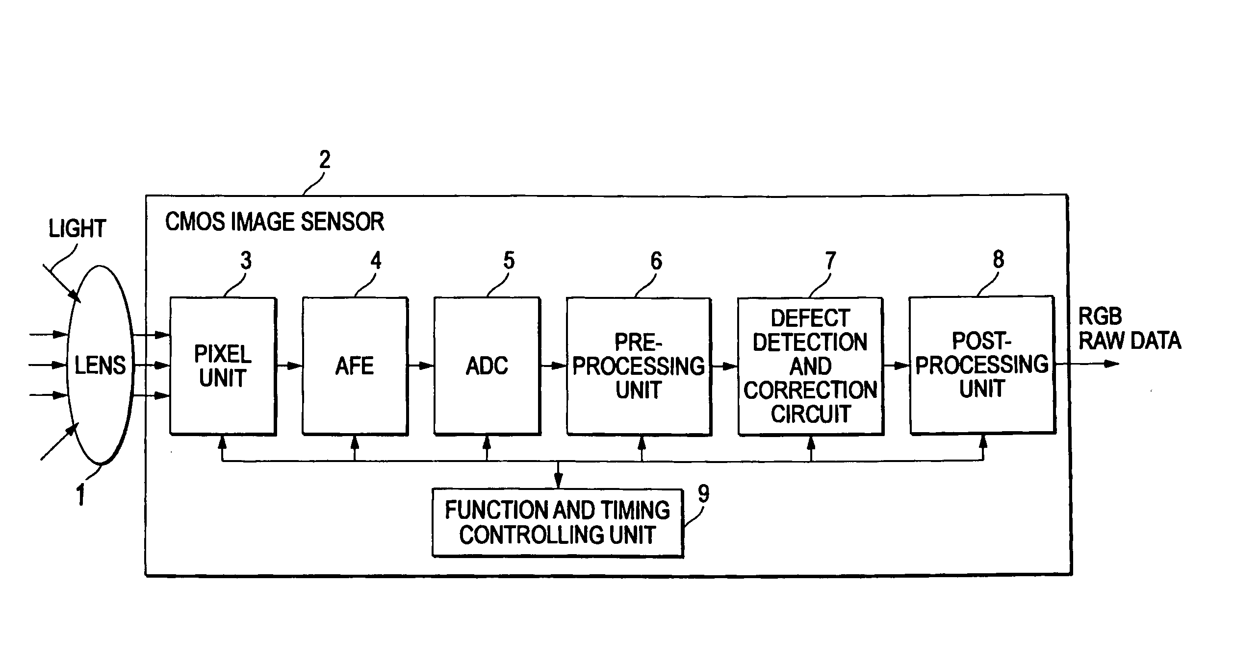
[0031]FIG. 1 is a diagram showing a configuration of the image sensor according to the first embodiment of this invention.

[0032] As shown in FIG. 1, the image sensor of the first embodiment is a CMOS image sensor 2, for example, which is a solid-state image pickup element. The image sensor 2 is used for converting light made incident through a lens 1 for forming an image of a subject of an image pickup device into pixel signals (electric signals) and provided with a pixel unit 3, an AFE (Analog Front End) 4, an ADC (Analog to Digital Converter) 5, a pre-processing unit 6, a defect detection and correction circuit 7 realizing a defective pixel detection and correction method of this invention, a post-processing unit 8, and a function and timing controlling unit 9.

[0033] The incident light obtained from the subject is input into the pixel unit 3 of ...

second embodiment

[0090]FIG. 6 is a diagram showing a configuration of a defect detection and correction circuit of an image sensor according to a second embodiment.

[0091] As shown in FIG. 6, the image sensor of the second embodiment is the same as the CMOS image sensor 2 of the first embodiment except for using the defect detection and correction circuit 60 in place of the defect detection and correction circuit 7. Other components are the same as those of the CMOS image sensor 2 of the first embodiment, and descriptions thereof are omitted.

[0092] The defect detection and correction circuit 60 has a defect detection coefficient calculation unit 61, a reference pixel calculation unit 62, a pixel level calculation unit 63, a threshold value calculation unit 64, a third defect processing and judgment unit 65, a fourth defect processing and judgment unit 66, a pixel distribution calculation unit 67, a first defect correction amount calculation unit 68, a second defect correction amount calculation uni...


PUM


Abstract

An image sensor is disclosed, which includes: a pixel unit having a plurality of pixels each outputting incident light as a pixel signal; an amplifier amplifying the pixel signal output from the pixel unit; and a defective pixel detection circuit performing a defective pixel detection on signals output from the amplifier, wherein the defective pixel detection circuit adjusts the detection accuracy of the defective pixel detection in accordance with an exposure condition of the pixel unit.

Description

CROSS REFERENCE TO RELATED APPLICATIONS [0001] The present invention contains subject matter related to Japanese Patent Application JP 2004-189207 filed in the Japanese Patent Office on Jun. 28, 2004, the entire contents of which being incorporated herein by reference. BACKGROUND OF THE INVENTION [0002] 1. Field of the Invention [0003] This invention relates to an image sensor capable of detecting and correcting a defective pixel without having a storage unit for storing an address of the defective pixel. [0004] 2. Description of the Related Art [0005] In a solid-state pickup element formed on a semiconductor substrate, such as a CMOS image sensor and a CCD (Charge Coupled Device) image sensor, a defective pixel is generated in some cases due to a local crystal defect and the like on the semiconductor substrate. Since a signal level output from such defective pixel is specific to the defective pixel and independent from an amount of incident light, quality of a picked up image can u...

Claims


Application Information

Patent Timeline
Patent Type & Authority Applications(United States)
IPC IPC(8): H04N9/64H04N5/335H04N5/367H04N5/369H04N5/374
CPCH04N5/367H04N25/68
Inventor IZUMI, DAISAKUHARUTA, TSUTOMUMAKINO, EIJI
Owner SONY SEMICON SOLUTIONS CORP
Why Eureka
Try Eureka