
Creating a dielectric layer using ALD to deposit multiple components

a dielectric layer and ald technology, applied in the field of dielectric layers, can solve the problems of difficult manufacturing of barriers, difficult fabrication of triangular barriers, and inability to meet the requirements of the proposed solution

Inactive Publication Date: 2006-01-12
SANDISK TECH LLC
View PDF45 Cites 14 Cited by
  • Summary
  • Abstract
  • Description
  • Claims
  • Application Information

AI Technical Summary

Benefits of technology

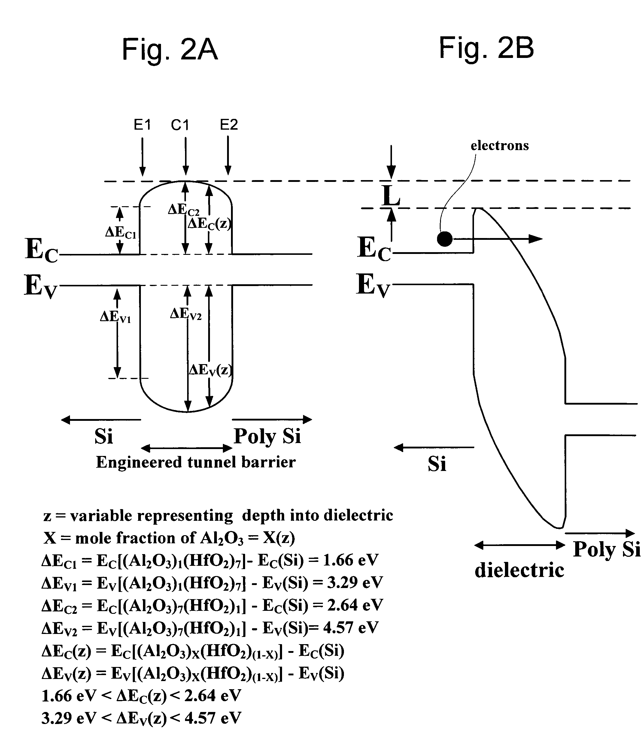
The patent describes a method for creating a dielectric layer with a rounded bottom of a conduction band profile for use in electronic devices such as flash memory devices. The method involves depositing multiple components using atomic layer deposition, where the mole fractions of the components change as a function of depth in the layer. The resulting dielectric layer has a rounded bottom of a conduction band profile that can improve performance and reliability of the electronic device. The method can be used with various types of flash memory devices and other non-volatile memory devices.

Problems solved by technology

However, such a proposal is not optimal.
Furthermore, an author of Likharev I and Likharev II specifically suggests that such a triangular barrier may have fabrication issues.
Similarly, the '654 patent proposes a tunnel barrier dielectric layer with a round shaped bottom of a conduction band profile; however, the '654 patent admits that such a barrier may be difficult to manufacture.

Method used


Image

  • Creating a dielectric layer using ALD to deposit multiple components
  • Creating a dielectric layer using ALD to deposit multiple components
  • Creating a dielectric layer using ALD to deposit multiple components

Examples


Embodiment Construction

[0044] The invention is illustrated by way of example, and not by way of limitation, in the figures of the accompanying drawings in which like references indicate similar elements. It should be noted that references to an or one embodiment in this disclosure are not necessarily the same embodiment, and such references mean at least one.

[0045] In the following description, various aspects of the present invention will be described. However, it will be apparent to those skilled in the art that the present invention may be practiced with only some or all of the aspects of the present disclosure. For purposes of explanation, specific numbers, materials and configurations are set forth in order to provide a thorough understanding of the invention. However, it will be apparent to one skilled in the art that the present invention may be practiced without all of the specific details. In other instances, well known features are omitted or simplified in order not to obscure the present inven...


PUM


Abstract

A dielectric layer is created for use with non-volatile memory and / or other devices. The dielectric layer is created using atomic layer deposition to deposit multiple components whose mole fractions change as a function of depth in the dielectric layer in order to create a rounded bottom of a conduction band profile for the dielectric layer.

Description

[0001] This application is a continuation-in-part application of U.S. patent application Ser. No. 10 / 762,181, entitled “Non-Volatile Memory Cell Using High-K Material and Inter-Gate Programming,” filed Jul. 17, 2003, incorporated herein by reference in its entirety.CROSS-REFERENCE TO RELATED APPLICATIONS [0002] The following applications are cross-referenced and are incorporated by reference herein in their entirety: [0003] U.S. patent application Ser. No. ______ [Attorney Docket No. SAND-01074US0], entitled “ATOMIC LAYER DEPOSITION WITH NITRIDATION AND OXIDATION,” inventor Nima Mokhlesi, filed the same day as the present application; and [0004] U.S. patent application Ser. No. ______ [Attorney Docket No. SAND-01022US1], entitled “DIELECTRIC LAYER CREATED USING ALD TO DEPOSIT MULTIPLE COMPONENTS,” inventor Nima Mokhlesi, filed the same day as the present application. BACKGROUND OF THE INVENTION [0005] 1. Field of the Invention [0006] The present invention relates to dielectric layer...

Claims


Application Information

Patent Timeline
Patent Type & Authority Applications(United States)
IPC IPC(8): H01L21/336H01L21/31G11C16/04H01L21/8247H01L29/423H01L29/51H01L29/788
CPCH01L27/115H01L27/11521H01L29/7881H01L29/513H01L29/66825H01L29/42324H01L29/40114H10B69/00H10B41/30
Inventor MOHKLESI, NIMA
Owner SANDISK TECH LLC
Learn More