MOS transistor having a recessed gate electrode and fabrication method thereof

a technology of metal oxide semiconductor and gate electrode, which is applied in the direction of transistors, semiconductor devices, electrical equipment, etc., can solve the problems of degrading the refresh property of the dram device, short channel effect, and typically reduced channel length of the mos transistor

Inactive Publication Date: 2006-01-26
SAMSUNG ELECTRONICS CO LTD
View PDF14 Cites 43 Cited by
  • Summary
  • Abstract
  • Description
  • Claims
  • Application Information

AI Technical Summary

Benefits of technology

[0014] It is therefore a feature of an embodiment of the present invention to provide a MOS transistor having a recessed gate electrode, and a fabrication method thereof, that may avoid unnecessarily reducing the size of an active area of the transistor.

Problems solved by technology

As a result, the channel length of the MOS transistors is typically reduced, which may cause a short channel effect.
When the short channel effect occurs in an access MOS transistor employed as a memory cell in a DRAM device, a threshold voltage of the DRAM cell decreases and leakage current increases, which degrades a refresh property of the DRAM device.
However, the decreased gate size may result in misalignment, and a metal silicide layer formed on the polysilicon may be cracked when the surface of the metal silicide layer is not uniform.

Method used


Image

  • MOS transistor having a recessed gate electrode and fabrication method thereof
  • MOS transistor having a recessed gate electrode and fabrication method thereof
  • MOS transistor having a recessed gate electrode and fabrication method thereof

Examples


Embodiment Construction

[0033] Korean Patent Application No. 2004-57855, filed Jul. 23, 2004, in the Korean Intellectual Property Office, and entitled: “MOS Transistor Having a Recessed Gate Electrode and Fabrication Method Thereof,” is incorporated herein by reference in its entirety.

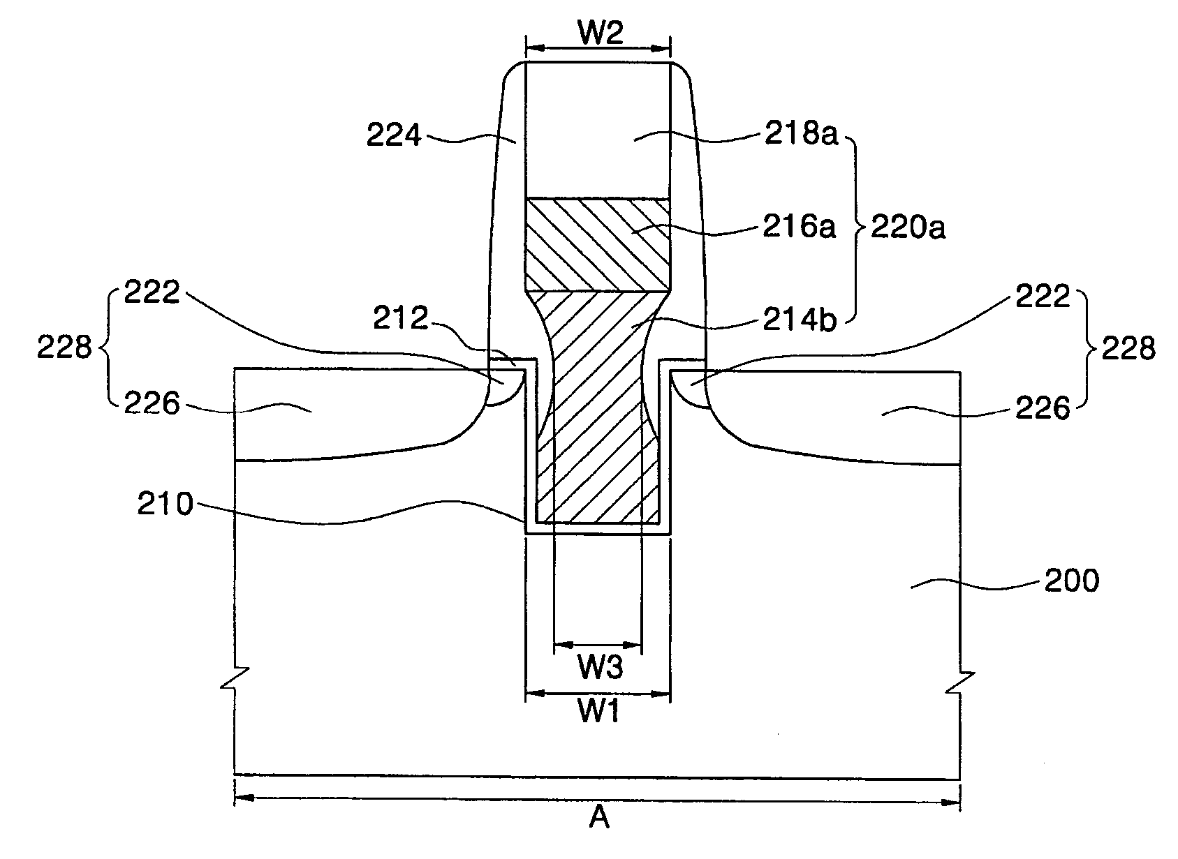
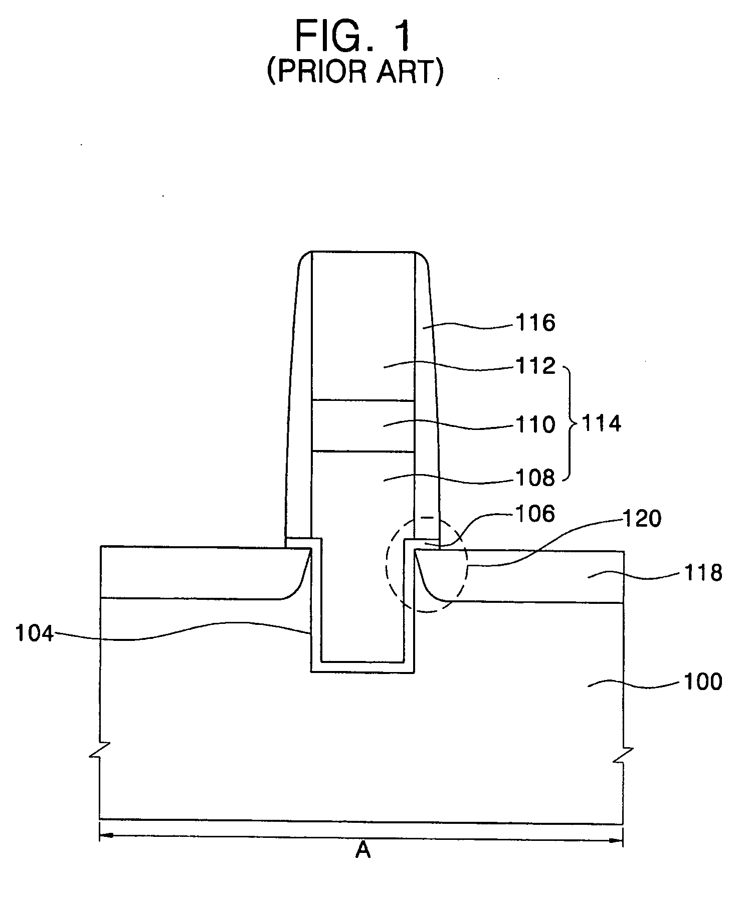
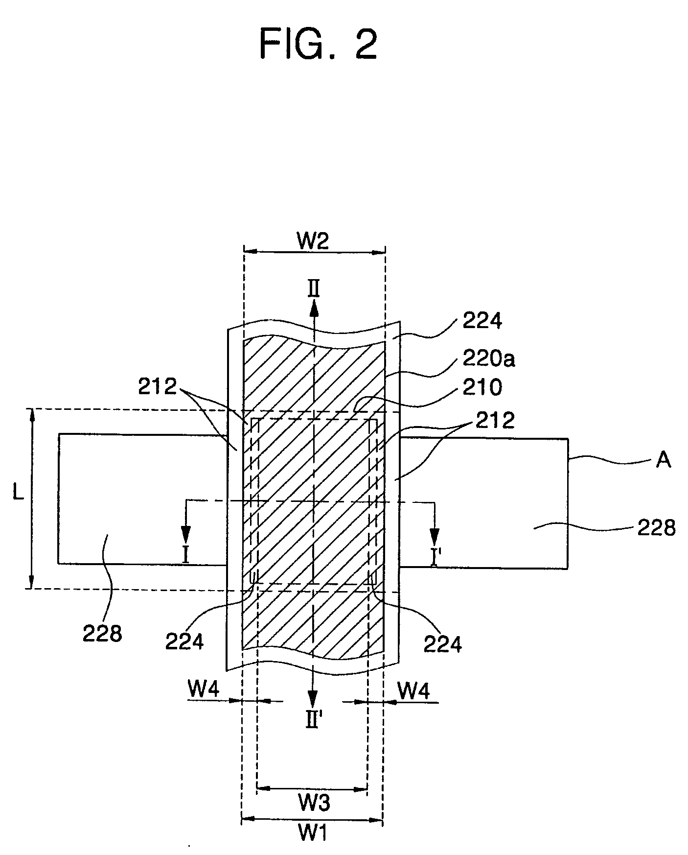
[0034] The present invention will now be described more fully hereinafter with reference to the accompanying drawings, in which exemplary embodiments of the invention are shown. The invention may, however, be embodied in different forms and should not be construed as limited to the embodiments set forth herein. Rather, these embodiments are provided so that this disclosure will be thorough and complete, and will fully convey the scope of the invention to those skilled in the art. It will also be understood that when a layer is referred to as being “on” another layer or substrate, it can be directly on the other layer or substrate, or intervening layers may also be present. Further, it will be understood that when a layer is ...


PUM


Abstract

A metal oxide semiconductor (MOS) transistor having a recessed gate electrode and a fabrication method thereof are provided. The MOS transistor includes a semiconductor substrate and an isolation layer formed in a predetermined region of the semiconductor substrate to define an active region. A channel trench region is disposed within the active region to cross the active region. A gate insulating layer is disposed to cover sidewalls and a bottom of the channel trench region. The MOS transistor has a gate pattern that fills the channel trench region and crosses above the active region. A portion of the sidewall of the gate pattern is recessed at an upper corner of the channel trench region and has a width smaller than the width of the top of the gate pattern and smaller than the width of the channel trench region.

Description

BACKGROUND OF THE INVENTION [0001] 1. Field of the Invention [0002] The present invention relates to a semiconductor device and a fabrication method thereof, and more particularly, to a metal oxide semiconductor (MOS) transistor having a recessed gate electrode and a fabrication method thereof. [0003] 2. Description of the Related Art [0004] Increases in the integration density of semiconductor memory devices such as dynamic random access memory (DRAM) are typically accompanied by corresponding decreases in the area occupied by MOS transistors in the devices. As a result, the channel length of the MOS transistors is typically reduced, which may cause a short channel effect. When the short channel effect occurs in an access MOS transistor employed as a memory cell in a DRAM device, a threshold voltage of the DRAM cell decreases and leakage current increases, which degrades a refresh property of the DRAM device. Accordingly, a MOS transistor having a recessed gate electrode capable of...

Claims


Application Information

Patent Timeline
Patent Type & Authority Applications(United States)
IPC IPC(8): H01L21/336H01L29/80H01L29/94H01L21/3205
CPCH01L21/28114H01L27/10876H01L29/7834H01L29/66621H01L27/10891H10B12/053H10B12/488H01L29/66348H01L29/66613H01L29/8128
Inventor PAIK, JAE-CHOEL
Owner SAMSUNG ELECTRONICS CO LTD
Why Eureka
Try Eureka