CMOS negative resistance/Q enhancement method and apparatus

a negative resistance and enhancement technology, applied in the field of negative resistance circuits, to achieve the effect of optimizing the quality factor q

Inactive Publication Date: 2006-01-26
THE TRUSTEES OF COLUMBIA UNIV IN THE CITY OF NEW YORK
View PDF4 Cites 14 Cited by
  • Summary
  • Abstract
  • Description
  • Claims
  • Application Information

AI Technical Summary

Benefits of technology

[0023] A gate of the NMOS transistor from the first pair of transistors and a gate of the NMOS transistor from the second pair of transistors are capacitively cross-coupled with inputs to the resonators. A second control voltage biases the gate of the NMOS transistor of the first pair of transistors through a third bias resistor, and the gate of the NMOS transistor of the second pair of transistors through a fourth bias resistor. Although not shown in the figures for this embodiment, the optimizing circuit may employ a separate biasing voltage for each of the NMOS transistors. A gate of the NMOS transistor from the first pair of transistors is capacitively coupled to a ground reference voltage, and a gate of the NMOS transistor from the second pair of transistors is capacitively coupled to the ground reference voltage.
[0024] The optimizing circuit also includes a current source for providing a controlled current to the transistors in the CMOS configuration. The current source includes a fifth transistor electrically coupled in series with the transistor pairs in the CMOS configuration, between a supply voltage and a ground reference voltage, so that a current-control voltage applied to the fifth transistor controls current flowing through the transistor pairs in the CMOS configuration.
[0025] A method of optimizing a quality factor Q associated with an electrical resonator system includes providing a negative resistance, generated by an optimizing circuit, electrically coupled to a resonator circuit. The resonator circuit includes an inductor and a capacitor, and the optimizing circuit includes at least one pair of NMOS or one pair PMOS transistors with gates cross-coupled with inputs to the resonator through capacitors. The method further includes adjusting one or more control voltages applied to the optimizing circuit so as to substantially optimize the quality factor Q associated with the resonator circuit. The method further includes measuring the quality factor Q and providing a control system that adjusts the one or more control voltages as a function of the measured Q
[0026] A circuit for providing a negative resistance across a first input and a second input includes a first CMOS transistor pair arranged in parallel with a second CMOS transistor pair, and a current source for controlling the current flowing through the transistor pairs in the CMOS configurations. The first CMOS transistor pair is capacitively cross-coupled with the first and second inputs, and includes a first PMOS transistor and a first NMOS transistor with their drains electrically connected. The second CMOS transistor pair is capacitively cross-coupled with the first and second input, and includes a second PMOS transistor and a second NMOS transistor with their drains electrically connected. The second CMOS pair is arranged in parallel with the first CMOS pair such that the source of the first PMOS transistor is electrically coupled to the source of the second PMOS transistor, and the source of the first NMOS transistor is electrically coupled to the source of the

Problems solved by technology

In some cases the quality factor Q may need to be balanced against certain tradeoffs with respect to the circuit or overall s

Method used


Image

  • CMOS negative resistance/Q enhancement method and apparatus
  • CMOS negative resistance/Q enhancement method and apparatus
  • CMOS negative resistance/Q enhancement method and apparatus

Examples


Embodiment Construction

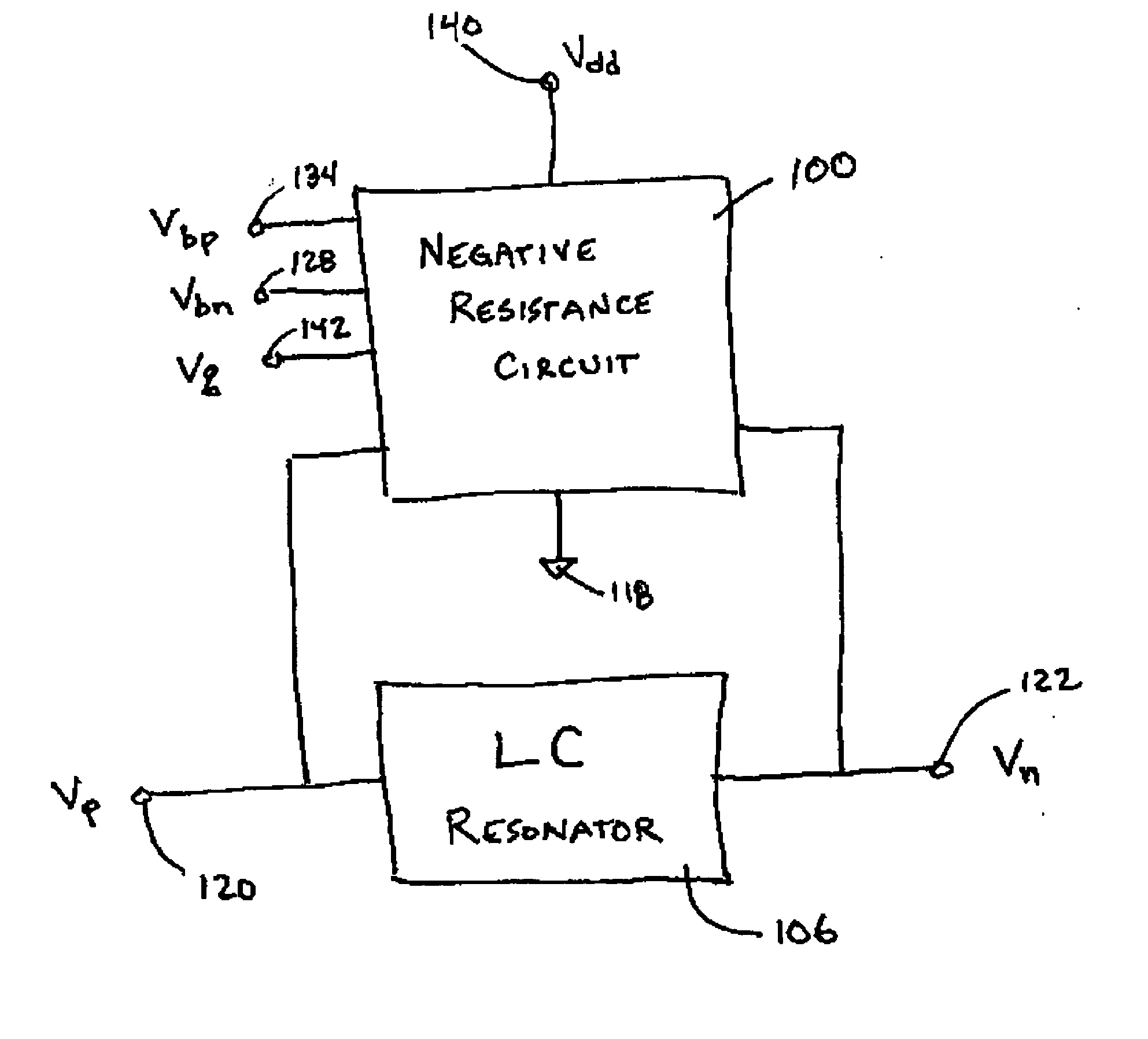
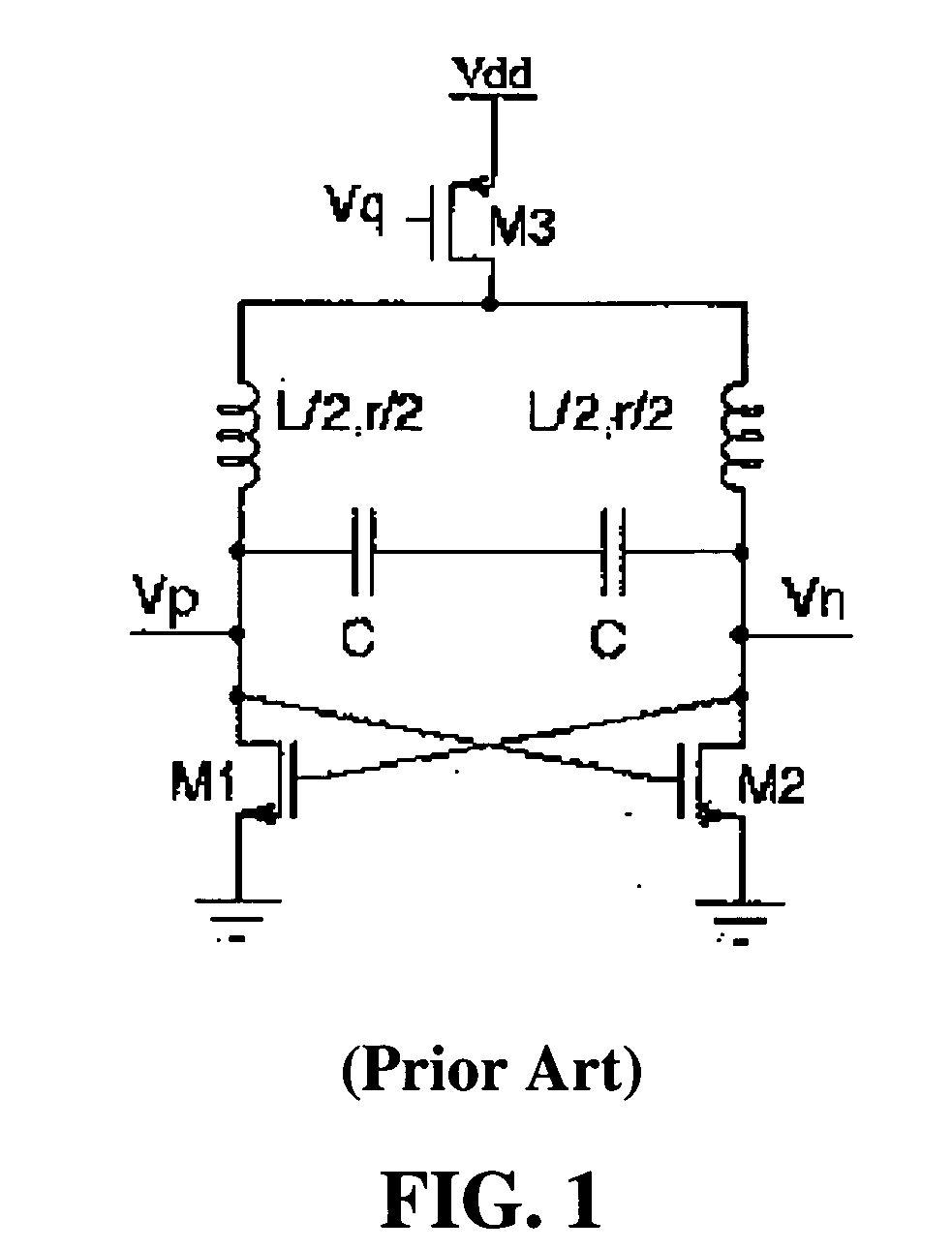
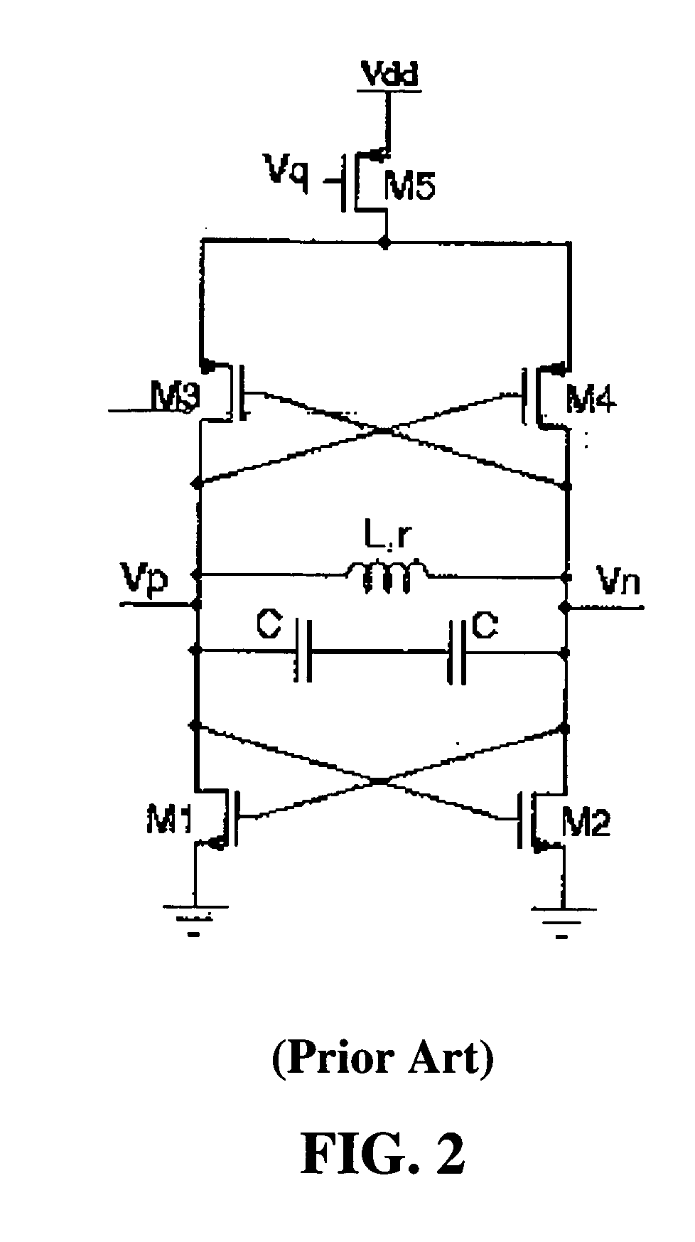
[0036] One embodiment of a CMOS negative resistance circuit 100 is shown in FIG. 4, coupled in parallel to an LC resonator 106. FIG. 5 shows an expanded view of the negative resistance circuit 100 and the LC resonator 106 of FIG. 4. The capacitor C 102 and the inductor L 104 form a parallel LC resonator 106. The inductor 104 is a lossy device; the lossy component is typically modeled as a resistance connected in series with the inductance. FIG. 5 shows the presence of that resistance via the “r” in the inductor symbol. The remaining components in FIG. 5 represent a negative resistance circuit applied to the resonator to cancel the loss. M1110 and M2112 are NMOS transistors; M3114 and M4116 are PMOS transistors. The drains of M1110 and M3114 are electrically coupled together (referred to herein as a “drain coupling” of these transistors), and the drains of M2112 and M4116 are electrically coupled together. The sources of M3114 and M4116 are electrically coupled together, and the sour...


PUM


Abstract

An apparatus for optimizing a quality factor Q associated with an electrical resonator system includes an LC resonator and an optimizing circuit for providing a negative resistance. The optimizing circuit is electrically coupled to the resonator circuit, and includes two CMOS transistor pairs with the gates of the PMOS transistors cross-coupled with inputs to the resonator through capacitors, and the gates of the NMOS transistor cross-coupled with the inputs to the resonator through capacitors. The optimizing circuit receives at least one control voltage for varying the negative resistance by selectively biasing the PMOS transistors and NMOS transistors. The optimizing circuit also includes a current source for providing a controlled current to the CMOS transistor pairs. The current source is situated either between a supply voltage and the CMOS transistor pairs, or between the CMOS transistor pairs and a ground reference voltage. A current-control voltage controls the current flowing through the CMOS transistor pairs.

Description

BACKGROUND OF THE INVENTION [0001] The present invention relates to negative resistance circuits, and more particularly, to Q enhancement of LC filters and resonators using tuning circuits that incorporate a negative resistance. [0002] A circuit that realizes a negative resistance has many useful applications. For example, in a practical LC filter or resonator circuit, the inductor L is lossy to some extent. This loss may be modeled as a real, positive resistance component in series with the pure inductance component of the physical inductor. The quality factor (referred to herein as “Q”) of the LC filter or resonator is inversely proportional to this loss, i.e., the Q decreases as the resistance value increases. It is well known in the art to combine a negative resistance with the inductor to reduce or eliminate the loss component, thereby optimizing the Q. [0003] LC resonators fabricated on analog integrated circuits (ICs) typically do not exhibit a predictable Q. The processing v...

Claims


Application Information

Patent Timeline
IPC IPC(8): H03B5/12
CPCH03B2201/036H03B5/124H03B5/1212H03B5/1228
Inventor STANIC, NEBOJSATSIVIDIS, YANNIS
Owner THE TRUSTEES OF COLUMBIA UNIV IN THE CITY OF NEW YORK
Why Eureka
Try Eureka