
Single poly non-volatile memory

a non-volatile memory, single-poly technology, applied in semiconductor devices, digital storage, instruments, etc., can solve the problems of large coupling area (p diffusion region—floating gate), complicating the cell fabrication process, and cell performance such as programming speed is still not satisfactory, so as to achieve faster program speed and lower current consumption

Active Publication Date: 2006-01-26
EMEMORY TECH INC
View PDF6 Cites 43 Cited by
  • Summary
  • Abstract
  • Description
  • Claims
  • Application Information

AI Technical Summary

Benefits of technology

[0012] It is the primary object of the present invention to provide an erasable programmable non-volatile memory cell structure with the characteristics of faster program speed and lower current consumption while programming the cell.

Problems solved by technology

One disadvantage of this approach is that a large coupling area (P diffusion region—floating gate) is required.
However, the cell structure needs a limiting tunneling window, which complicates the fabrication process of the cell.
Although the 2-T EPROM (Neobit™) technology disclosed in the commonly owned U.S. Pat. No. 6,678,190 has several advantages in terms of, for example, cell size and CMOS process compatibility, over other prior arts, the cell performance such as programming speed is still not satisfactory yet.

Method used


Image

  • Single poly non-volatile memory
  • Single poly non-volatile memory
  • Single poly non-volatile memory

Examples


Embodiment Construction

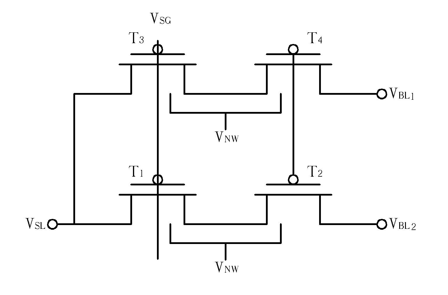
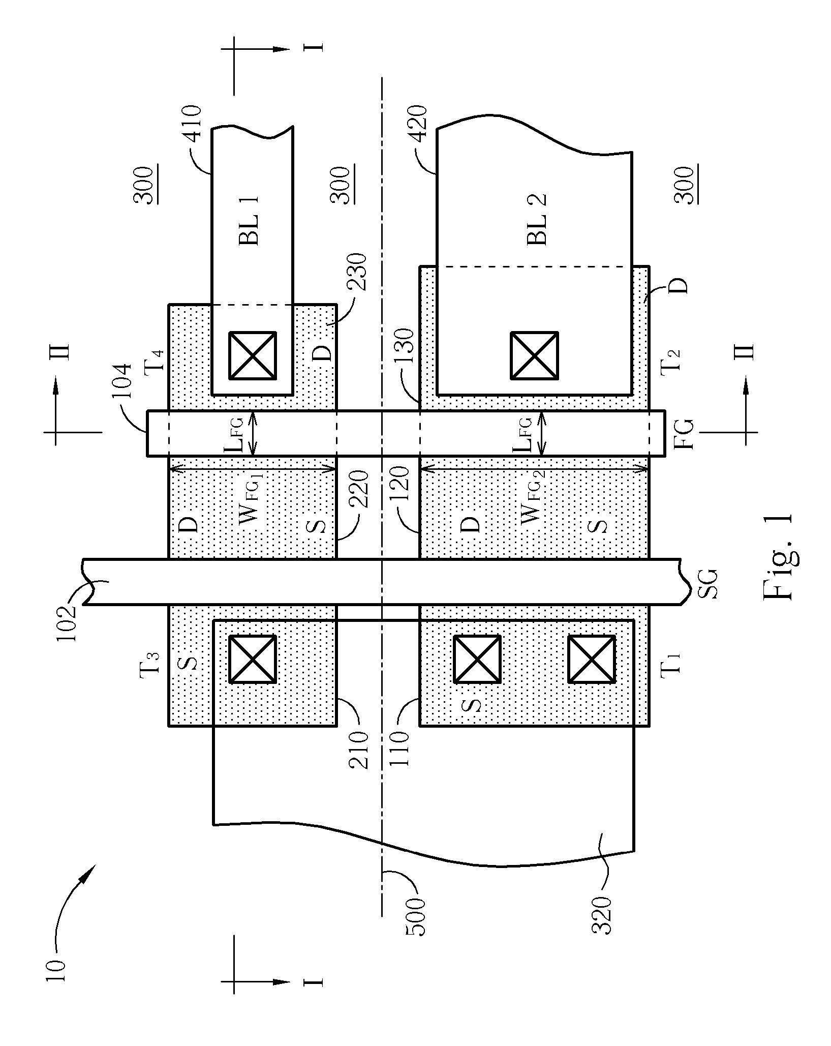
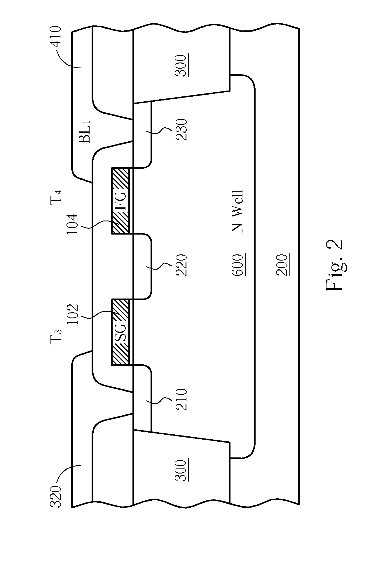
[0023] The present invention pertains to an erasable programmable non-volatile memory cell, which is capable of being programmed at a relatively faster programming speed. According to this invention, the current consumption for programming one cell is reduced. Preferred embodiments in accordance with this invention will now be discussed with reference to FIG. 1 to FIG. 9. It shall be appreciated that, in some of the figures or tables demonstrated in the specification, the abbreviation “PGM” refers to “program” or “programming”.

[0024] Please refer to FIG. 1 to FIG. 3, wherein FIG. 1 is an enlarged top view schematically showing 4-T (four-transistor) cell unit layout of an non-volatile memory device in accordance with one preferred embodiment of the present invention; FIG. 2 is a schematic cross-sectional diagram illustrating the cell unit 10 taken along line I-I; FIG. 3 is a schematic cross-sectional diagram illustrating the cell unit 10 taken along line II-II. As shown in FIG. 1, t...


PUM


Abstract

An erasable programmable non-volatile memory cell encompasses an ion well; a first select transistor including a select gate, source / drain formed in the ion well, and a channel region formed between its source and drain; a first floating gate transistor having a drain, a source coupled to the drain of the first select transistor, a first floating gate channel region formed between its drain and source, and a common floating gate overlying the floating gate channel region; a second select transistor including a select gate, source / drain formed in the ion well, and a channel region formed between its source and drain; and a second floating gate transistor having a drain, a source coupled to the drain of the second select transistor, a second floating gate channel region formed between its drain and source, and the common floating gate overlying the second floating gate channel region.

Description

CROSS REFERENCE TO RELATED APPLICATIONS [0001] This application claims the benefit of U.S. provisional application No. 60 / 521,916, filed Jul. 20, 2004.BACKGROUND OF INVENTION [0002] 1. Field of the Invention [0003] The present invention relates to non-volatile memory devices and, more particularly, to a single-poly erasable programmable non-volatile memory cell with the characteristics of faster program speed and lower current consumption while programming the cell. [0004] 2. Description of the Prior Art [0005] A single-poly electrically programmable read-only-memory (EPROM) cell is a non-volatile storage device which is suggested to be fabricated by process steps fully compatible with conventional single-poly CMOS fabrication process. As a result, single-poly EPROM cells are often embedded in CMOS logic and mixed-signal circuits. [0006] Conventional single-poly EPROM cells utilize a well region as the control gate of the cell, and further utilize adjoining N+ and P+ contact regions...

Claims


Application Information

Patent Timeline
IPC IPC(8): G11C16/04
CPCH01L27/115G11C16/0441H10B69/00
Inventor CHEN, HSIN-MINGWANG, SHIH-CHENTSAI, HONG-PING
Owner EMEMORY TECH INC
Learn More