Patterned strained semiconductor substrate and device

a technology of strained and non-strained areas, applied in the direction of semiconductor devices, electrical equipment, basic electric elements, etc., can solve the problems of strained silicon layer, multi-layered sige layer, and a large amount of silicon layer,

Active Publication Date: 2006-01-26
TAIWAN SEMICON MFG CO LTD
View PDF99 Cites 127 Cited by
  • Summary
  • Abstract
  • Description
  • Claims
  • Application Information

AI Technical Summary

Problems solved by technology

The problem with this approach is that it requires a very thick, multilayered SiGe layer.
Additionally, the misfit dis-locations formed between the SiGe layer and the epitaxial silicon layer are random, highly non-uniform in density, and fairly uncontrollable due to heterogeneous nucleation that cannot be easily controlled.
Consequently, the physical stress applied to the silicon layer is apt to be defective.
At locations where misfit density is high, d

Method used


Image

  • Patterned strained semiconductor substrate and device
  • Patterned strained semiconductor substrate and device
  • Patterned strained semiconductor substrate and device

Examples


Embodiment Construction

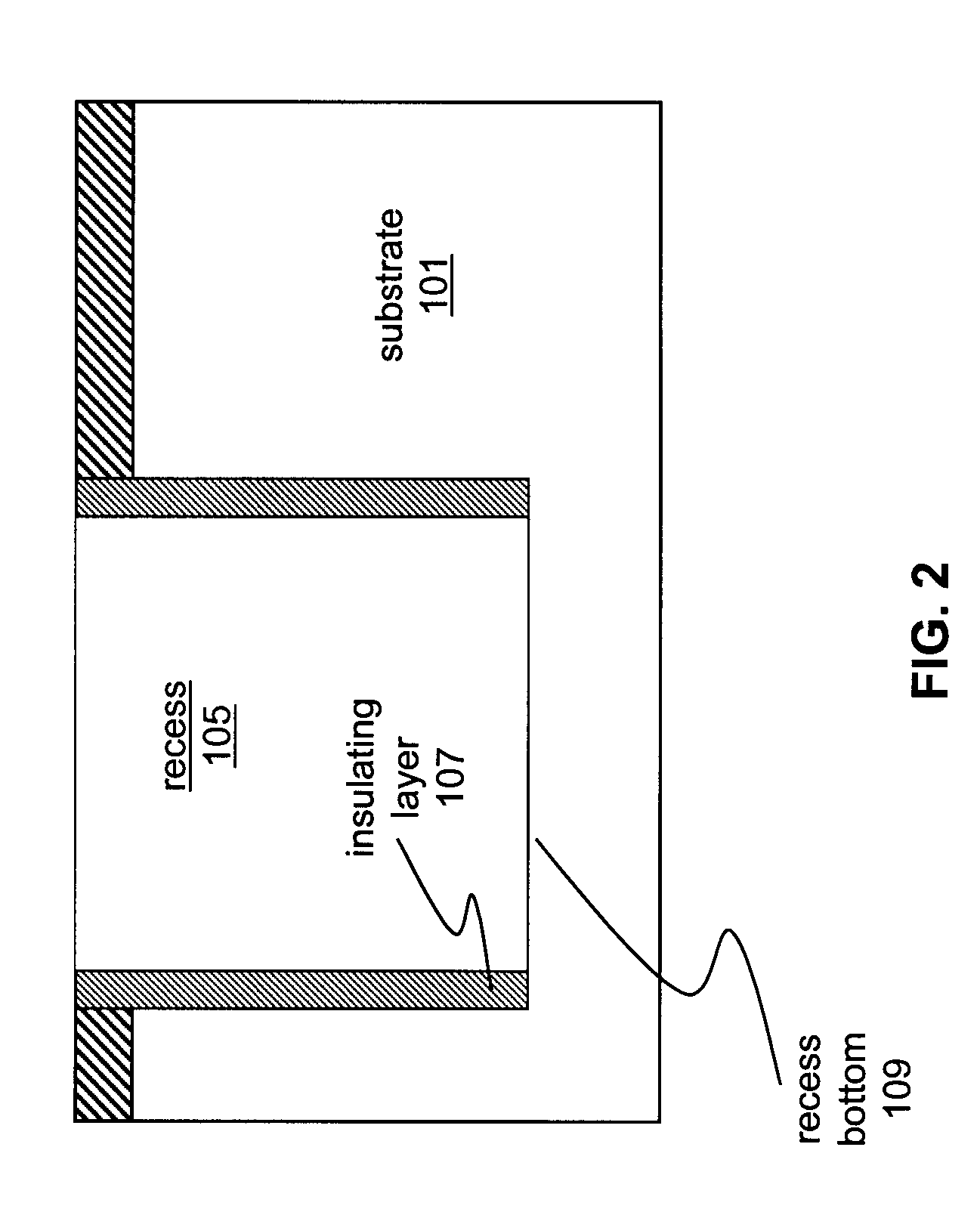
[0029] The invention is directed to an electrical, digital, semiconductor, or other device having a substrate on which a pattern of strained and non-strained (i.e., relaxed) materials are formed. The strained material may be placed in tension or compression due to a lattice constant / structure difference with an underlying layer of relaxed material. In turn, the relaxed material is formed on a buffer layer, which contacts a portion of the substrate.

[0030] A material forming the buffer layer varies in concentration throughout the layer, and has a lattice constant / structure mismatch with the material that forms the substrate. Because the material forming the buffer layer increases in concentration the further the buffer layer extends from the substrate, defects normally caused by the lattice mis-match are virtually eliminated. The formation of the relaxed layer on the buffer layer further reduces and / or eliminates defects to such an extent that the strained material is virtually free ...


PUM


Abstract

A method that includes forming a pattern of strained material and relaxed material on a substrate; forming a strained device in the strained material; and forming a non-strained device in the relaxed material is disclosed. In one embodiment, the strained material is silicon (Si) in either a tensile or compressive state, and the relaxed material is Si in a normal state. A buffer layer of silicon germanium (SiGe), silicon carbon (SiC), or similar material is formed on the substrate and has a lattice constant/structure mis-match with the substrate. A relaxed layer of SiGe, SiC, or similar material is formed on the buffer layer and places the strained material in the tensile or compressive state. In another embodiment, carbon-doped silicon or germanium-doped silicon is used to form the strained material. The structure includes a multi-layered substrate having strained and non-strained materials patterned thereon.

Description

BACKGROUND OF INVENTION [0001] The invention relates to methods and structures for manufacturing semiconductor devices having improved device performances, and more particularly, to methods and structures for forming patterns of strained and non-strained areas on a substrate. [0002] Emerging technologies, such as embedded Dynamic Random Access Memory (eDRAM), Application Specific Integrated Circuits (ASIC), and system-on-chip (SoC), require the combination of high-performance logic devices and memory devices on the same chip. It is also desired to have digital circuits and analog circuits on the same chip for some applications. It has been shown that logic devices exhibit better performance when formed on a tensily strained silicon layer that is epitaxially grown on another epitaxially grown silicon germanium (SiGe) layer that has been relaxed. [0003] A fully relaxed SiGe layer has a lattice constant which is larger than that of silicon. Thus, when the silicon layer is epitaxially g...

Claims


Application Information

Patent Timeline
IPC IPC(8): H01L21/76
CPCH01L21/823412H01L29/78687H01L29/739H01L29/1054
Inventor CHENG, KANGGUODIVAKARUNI, RAMACHANDRA
Owner TAIWAN SEMICON MFG CO LTD
Why Eureka
Try Eureka